Digital Signal Processing Filter Design Examples
IIR Design - Convert the band-pass analog filter with
transfer function:
![]()
which has a resonance (peak frequency response) at W = 4 to a digital filter using the bi-linear
transformation.
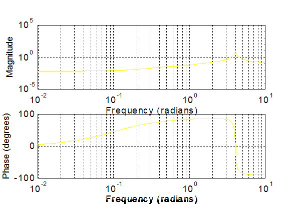
The digital filter is to have a resonance at w = p/2
A. What is the desired mapping?
Td = ½ to map W =
4 to
w
= p/2 using: ![]() or
or ![]()
The mapping is therefore: 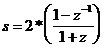
B. What is the resulting H(z)?
The resulting H(z) is:
![]()
C. Where are the poles and zeros of this filter?
Factoring the numerator gives the zeros and factoring the denominator yields the poles. The poles are approximately at 0.987e±jp/2 and the zeros are at -1 and 0.95
D. The Frequency Response of the digital filter (at a 1 kHz sample rate) is:
FIR Design - Starting with the ideal low-pass filter function with cutoff Wc = p/4 , develop an FIR low pass filter using a Hamming window that has the following characteristics:
wc = p/4 (cut off frequency)
M = 31 (Filter length)
A. What is the FIR filter pulse response? Sketch it below.
The pulse response is the product of sin(x)/x (the Inverse Fourier Transform of the ideal filter shifted to center at n=16) and the Hamming raised cosine window function.


B. What is the approximate transition width of the resulting filter?
The transition width for the rectangular window would be 1/T in normalized frequency, with the Hamming Window the Transition width is doubled to 2/T in normalized frequency.
C. Sketch the FIR filter frequency response below.
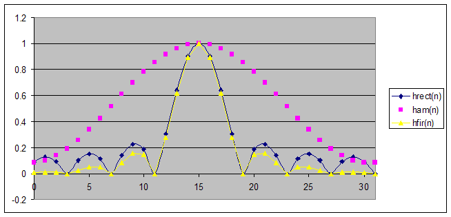
This is a low pass filter. The positive frequencies start at index 1 and go to index 16. The highest negative frequency is at index 17. DC (f=0) is at index 0 and 32.