FAIRFIELD UNIVERSITY
BEI School of Engineering
Electrical Engineering Department
SYLLABUS -
EE212- Computer Aided Circuit Analysis
Prerequisite:
Introduction to Circuits (or equivalent) 2
Credits 30 hours
Description: After a brief review of fundamental circuit
analysis techniques, both time and frequency domain analyses of passive and
active circuits are examined. Excel spreadsheets are used to aid in computation
and graphical plots. MicroSim PSpice or Electronic Workbench or a similar
application is used as the basic circuit analysis program. Use MatLab MathCAD to solve circuit problems
and plot results. The course focuses on
using four different computer programs to solve circuit analysis and design
problems. Comparisons are made to
assist the student in selecting the appropriate tool to accomplish a given
objective.
|
Instructor:
|
Jeffrey N. Denenberg
|
Email:
|
jdenenberg@fair1.fairfield.edu
|
|
Home Page:
|
http://pages.cthome.net/denenberg/
|
Phone:
|
(203) 268-1021(days &
eves.)
|
|
Textbook:
|
|
SW:
|
MatLab, Excel,
MathCAD, PSpice (MatLab and PSpice are supplied by instructor at no cost)
|
|
Pre-Requisites:
|
A first course in Circuit
Analysis
|
Exams:
|
Three (~4th , 9th
&14th wk) - 60%.
Comprehensive final - 40%
|
References:
1. Introduction
to Electric Circuits, Dorf & Svoboda,
1996, John Wiley & Sons. ISBN
0-471-12702-7
2. Electrical
Circuit Analysis 2nd Edition - Johnson,
Johnson & Hilburn - 1992 - Prentice Hall, ISBN 0-13-249335-7
3. Circuit
Analysis for Engineers, Mix & Schmitt
1985, John Wiley & Sons
4. Circuits,
Devices and Systems 5th Edition - Smith
& Dorf, John Wiley & Sons
Inc, 1992 ISBN
0-471-83944-2
|
|
Outcomes
|
Learning Goals
|
|
1.
|
Gain confidence with PCs for
engineering analysis purposes.
|
Use
Modern Engineering Tools
|
1.0
|
|
2.
|
Begin to understand computer
strengths and limitations
|
|
3. 3.
|
Gain familiarity with four
fundamental software applications MicroSim PSpice or Electronic Workbench,
EXCEL, MatLab and MathCAD
|
|
4.
|
Strengthen understanding of
basic circuit analysis techniques
|
Technical Content
|
0.5
|
|
5.
|
Apply Calculus to circuit
analysis problems
|
Math, Science &
Applications
|
0.5
|
Prepared By:
Dr. J. N. Denenberg June 10, 1999
|
Class
|
Topic
|
Text Reference
|
|
1.
|
Course Goals, Review
Kirchhoff’s Laws, Review Mesh & Nodal Analysis, Introduction to
MatLab
|
Chap 1, 2, 3
|
|
1.1.
|
Thevenin & Norton
Theorems
|
Chap. 4
|
|
2.
|
Phasor Analysis. Complex numbers. Use of EXCEL in solving
EE Problems - EXCEL Usage Lab
|
Chap 9
|
|
3.
|
Frequency Domain Analysis -
EXCEL Usage Lab
|
|
|
4.
|
Mid-term Exam. Operational Amplifiers
|
Chap 5
|
|
5.
|
MicroSim OR ELECTRONIC
WORKBENCH Introduction, Create & Edit Circuits. Examples RC Transient
& Frequency Analysis
|
|
|
5.1.
|
MicroSim OR ELECTRONIC
WORKBENCH (cont'd)- RLC (Resonance),
Notch Filter, Operational Amplifier - Lab
|
|
|
6.
|
Distribute Problem set and
begin analysis & design. - Lab
|
|
|
6.1.
|
Programming in MatLab
|
|
|
7.
|
Intro. to MathCAD - Lab
|
MathCAD Tutorial
|
|
8.
|
Examples of MathCAD
applications in EE - Lab
|
MathCAD & Notes
|
|
9.
|
Final Exam (Optional)
|
|
|
10.
|
If time permits: Transient Analysis Source Free
|
Chap 7, 8
|
The problem
set will consist of approximately ten problems to be solved using EXCEL,
PSPICE, and MathCAD or MatLab. At the
instructor’s option, the problem set may replace the Final Exam. Design problems will be included in the
problem set.
Grade
allocation: Problem set 60%
Midterm Exam 20%
Design Assignments 10%
Class Performance 10%
Total 100%
CLASS EXPECTATIONS
I. TEACHER
Distribute
syllabus.
Review
the material described in the syllabus.
Explain
material.
Identify
alternate reading assignments or books that clarify the material.
Relate
material to "real world" situations when possible.
Answer
questions.
Meet
at a mutually convenient time to discuss problems.
(I will be in the office on Thursday Evenings for the summer)
Be
receptive to new ideas.
Announce
business/class conflicts in advance.
Make
up missed classes.
Prepare
and administer 3 exams.
Grade
fairly.
Assign
appropriate home problems.
Homework
policy
Reviewed
in class
Collected
or not collected
Graded
or not
Quizzes
II. STUDENT
Ask
questions.
Stay
current.
Study
the material described in the syllabus.
Complete
the assigned homework.
Obtain
class notes and homework if a class is missed.
Use
the library to obtain supplemental material that explains an unclear topic.
Prepare
for exams.
Ask
for help.
ANTICIPATED POSTPONED
CLASS DATES
None
MAKEUP CLASS DATES
To be announced
1999 Class Meetings: May 24;
June 7, 14, 21, 28; July 5, 12, 19, 26; Final Exam: August 2.
Kirchoff’s Laws
1.
Voltage
1.1.
The Voltage around any closed path is zero.
or
1.2.
The sum of the voltage rises equals the sum of the voltage
falls around a closed path.
2.
Current
2.1.
The sum of the current at any node equals zero.
or
2.2.
The sum of the currents into a node equals the sum of the
current out of the node.
---------------------------------------------------------------------------------------------------------
Thevenin Equivalent Circuit
All circuits or portions of circuits can be replaced by a
Thevenin voltage source in series with a Thevenin impedance.
Do the following to perform this operation:
1. Calculate
the voltage at the points of interest to find the Thevenin equivalent voltage
source.
2. Thevenin
equivalent impedance -- Set all independent sources to zero by doing the
following: Short circuit all independent voltage sources and open circuit all
independent current sources. Then calculate the impedance at the points of interest
to find the Thevenin equivalent impedance.
Norton Equivalent Circuit
All circuits or portions of circuits can be replaced by a
Norton current source in parallel with a Norton admittance/impedance.
Do the following to perform this operation:
1. Short-circuit
the points of interest. Calculate the
current in the short circuit to find the Norton equivalent current source
value.
2. Norton
equivalent admittance/impedance -- Set all independent sources to zero by doing
the following: Short-circuit all independent voltage sources and open circuit all
independent current sources. Then calculate the admittance or impedance at the
points of interest to find the Norton equivalent admittance or impedance.
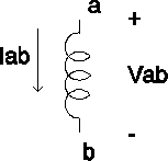
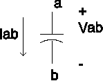
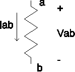
PASSIVE DEVICES
VIEW IMPEDANCE TIME FREQUENCY LAPLACE SERIES PARALLEL
DOMAIN DOMAIN DOMAIN
SUM SUM
--------------------------------------------------------------------------------------------------------------------------------------------------------------
--------------------------------------------------------------------------------------------------------------------------------------------------------------
--------------------------------------------------------------------------------------------------------------------------------------------------------------
H. Hoffman, 1/98
PASSIVE DEVICES
VIEW IMPEDANCE TIME FREQUENCY LAPLACE SERIES
PARALLEL
DOMAIN DOMAIN DOMAIN
SUM SUM
--------------------------------------------------------------------------------------------------------------------------------------------------------------
--------------------------------------------------------------------------------------------------------------------------------------------------------------
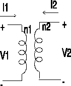
TRANSFORMER POWER
IN = POWER OUT
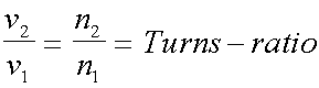

H. Hoffman, 1/98
FAIRFIELD UNIVERSITY
BEI School of Engineering
Electrical Engineering Department
EE 212 Computer Aided Circuit Analysis Typical
Problem Set
Take Home
========================================================================
All problems must be
submitted before the end of the term.
If the entire problem set is not submitted, the student will receive an
incomplete grade.
========================================================================
1. a) Find the transfer function (V2/V1) for the following bandpass filter . Use phasor notation.
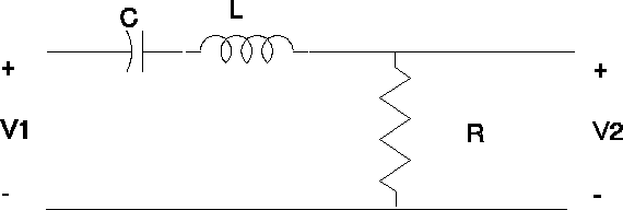
b) Determine the
magnitude and phase equations for the circuit.
c) Sketch the
magnitude and phase for component values:
R= 10 Ohms, L= 5
milliHenries, and C= 10 mF.
d) Confirm your sketch by using EXCEL to plot the magnitude
and phase
e) Again confirm
your sketch by using MicroSim or Electronic Workbench to plot the magnitude and
phase.
f) Apply a periodic square wave with the following characteristics to the input ( v1(t)
):
Rise & Fall time 10
nanosec
zero level 0
Volts
High level 15
Volts
Period 20
milli sec.
Use MicroSim or Electronic Workbench to find v2(t) .
g) For the same
periodic square wave described in part (f) , let R vary from 100 W to
1000 W
in steps of 100 W.
Again use MicroSim or Electronic Workbench to plot v2(t) for the different resistor values.
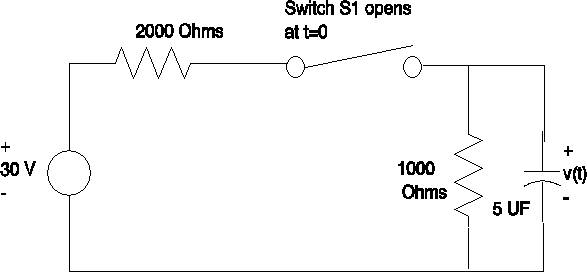
2. Assume switch S1
is closed for t<0. Find v(t) for
t>0.
3. a) Find the
transfer function (V2/V1) for the
following highpass filter. Assume an
ideal Operational amplifier.
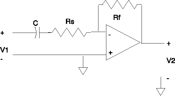
b) Determine the
magnitude and phase equations for the above circuit.
c) Sketch the
magnitude and phase with the following assumptions: Rf/Rs = 10, and 1/RsC =
1.
d) Select values of Rf, Rs, and C that will result in a
break point frequency of 1 Khz. Verify
your result by plotting the result using MicroSim or Electronic Workbench. Identify how you would determine the break
point frequency.
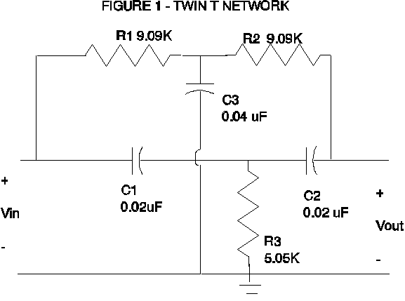
4. Plot the magnitude, magnitude in dB. and
phase versus of the parallel T filter circuit in Figure 1. Use the MicroSim or Electronic Workbench
program to compute the requested characteristics. Note that you will need a jumper connection, which may be found
as a connector in the component listing.
Carefully consider the frequency range over which to plot the response.
5. Given the
following homogenous differential equation that describes the natural response
for a circuit,
d2v dv
--- +
3 --- + 2
v = 0
dt2 dt
How many storage elements are there in the circuit?
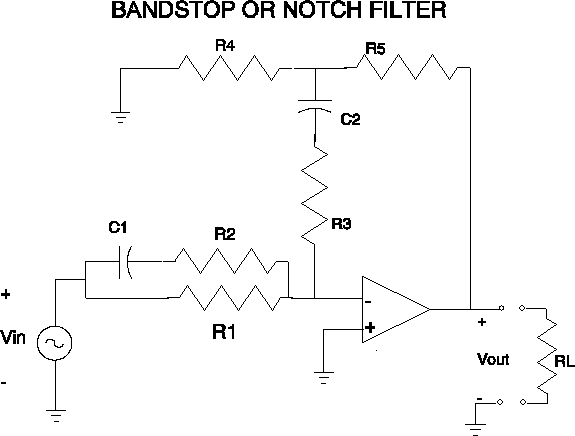
6. Design Problem #1
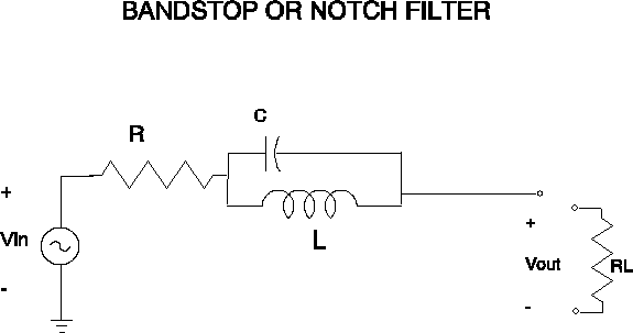
Consider a bandstop filter of the form shown above. Design a filter to reject a 60 Hz sinusoid
while passing other frequencies. The
bandwidth of the rejection desired is approximately 30 Hz., the load resistor
(RL ) is 600 W
, and resistor (R) is 600 W.
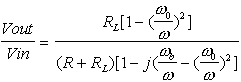
a) Show
that the transfer function Vout/Vin is
Vout/Vin
= RL / (R+Z+ RL) where Z is the impedance of the parallel
capacitor and inductor.
b) The
resonant frequency is 60 Hz. Using
phasor notation show that for w<< w0 and for w0 >> w
the transfer unction for Vout/Vin
is approximately RL
/ (R+ RL) .
c) Organize
the transfer function into the following format
where 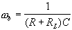
wb approximates the circuit bandwidth.
d) The
resonant frequency (w0
) is 60 Hz. Show that for w<< w0 and for
w0 >>
w the transfer function for Vout/Vin is approximately RL / (R+ RL).
e) Calculate
the capacitor and inductor values required to implement the 60 Hz bandstop
filter.
Using MicroSim or Electronic Workbench, verify the calculation by plotting the Magnitude
response. Also plot the phase response.
7. Design Problem #2
In the previous problem, the notch filter used only passive
elements. The passive circuit may
require the use of large, heavy, and expensive inductors. The active filter below uses resistors,
capacitors and op amps, but no inductors.
Select values of resistors and capacitors that will approximate a 60 Hz
notch filter and a 30 Hz bandwidth for the operational amplifier bandstop
filter. Use MicroSim or Electronic
Workbench to assist you in this exploration.
8. a) Using MathCAD, calculate and plot the magnitude and
phase functions for the RLC circuit
below . Let R=10 W
, L
= 5 milliHenries, and C = 5 mF.
Transfer Function =
V2/V1
b) Suppose we define
a Quality factor, Q ,where  . Express the transfer function for the series
resonant circuit as a function of Q,
. Express the transfer function for the series
resonant circuit as a function of Q,  , and w
. Show that the bandwidth is
, and w
. Show that the bandwidth is  . Recall that the resonant frequency is
  .
.
c) Suppose we wish to design a filter with a center
frequency of 1 Khz. and a bandwidth of 100 Hz.
Further assume that the load resistor, R, is 50 W. Select the values of L and C that will
provide the desired response. Plot the
magnitude of the transfer function. You
are at liberty to use any computer tools that you wish.