DORDT COLLEGE ENGINEERING DEPARTMENT
TEXTBOOK ERRATA
(last update 5/02/2013)
Sedra & Smith,
Microelectronic Circuits, 6th Ed.
ISBN-10 0-19-532303-3
ISBN-13 9780195323030
Oxford, 2010.
(link to errata for 5th edition)
This list was prepared from the first printing
of the textbook.
Some of these errata have been corrected in later printings,
which is easy to understand. Some additinal errata have been
accidentally introduced into later printings! Where I have
information on errata unique
to later printings, I have
included appropriate corrections.
Page 46, Problem 1.39 part (b)
Change "v = 10 μV" to
"vI = 10 μV"
(Posted 9/06/2012)
Page 112, Problem D2.34 part (d)
Add the word "Norton" so that part (d) reads as follows:
(d) If the amplifier is fed with a Norton current source
having a
current of 0.2 mA and a source resistance of
10 K , find
iL.
, find
iL.
Page 217, Figure P4.3 part (b)
The top diode should be labled D1 and
the bottom diode should be labeled D2.
(Posted 9/16/2010)
Page 220, Problem 4.22 Part (d)
Delete part (d) from the problem.
(It is a duplicate of Part(b))
(Posted 9/20/2010)
Page 226, Problem 4.75 Part (C)
Add, "during conduction" to part (c) so that it reads,
"(c) What is the average diode current during conduction?"
(Posted 10/21/2010)
Page 226, Problem 4.76.
In part (b) of the statement from problem 4.75, replace the
word "diode" with "rectifier." The problem then reads
(b) For what fraction of a cycle does the rectifier
conduct?
In part (c) add the phrase, "through each diode during
conduction." and delete one instance of the word "diode."
The question then reads. . .
(c) What is the average current through each diode
during conduction?
In part (d) add the phrase, "through each diode?" and delete
one instance of the word "diode." The question
then reads. . .
(d) What is the peak current through each diode?
Also see below for a clarification of this
problem.
Page 226, Problem 4.77.
In part (b) of the statement from problem 4.75, replace the
phrase, "does the diode conduct" with the phrase, "is there
conduction through the secondary winding of the transformer."
The problem then reads
(b) For what fraction of a cycle is there conduction through the
secondary winding of the transformer?
In part (c) add the phrase, "through each diode during
conduction." and delete one instance of the word "diode."
The question then reads. . .
(c) What is the average current through each diode during conduction?
In part (d) add the phrase, "through each diode?" and delete
one instance of the word "diode." The question then reads. . .
(d) What is the peak current through each diode?
Also see below for a clarification of this
problem.
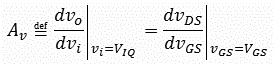
Page 270, Equation 5.35
The equation given is not the definition of
Av.
Change equation 5.35 to read as follows:
Page 327, Problem D5.5
Replace the last line of the problem statement with,
"maximum allowed VGS of 1.8 V."
(Posted 10/12/2012.)
Page 331, Problem 5.24
In the problem statement replace "(a)" with "(i)" and replace "(b)" with "(ii)." Leave the "(a)" and "(b)" in Figure P5.24 as thay are. There are two parts to the problem, part (i) and part (ii) and each of those parts needs to be considered once for (a) the n-channel MOSFET and once for (b) the p-channel MOSFET, a total of four things to consider.
(Posted 10/25/2012.)
Page 333, Problem 5.31
Add "in saturation" near the end of the first line of the problem statement so that the first line becomes,
"A particular MOSFET has VA = 50 V. For operation in saturation at"
(Posted 10/12/2012.)
Page 338, Problem 5.59.
In the first line of the problem statement delete the space between the number 2.5 and the "µp". Also, put the number in parenthesis. The first line then ends with this expression:
µnCox = (2.5)µpCox =
Better: just specify directly what is intended:µnCox = 20 µA/V2,
µpCox = 8 µA/V2
Also see the errata on the answer to problem 5.59
(As printed µnCox = 2.5 µA/V is a correct reading but that was not the author's intention.)Page 339, Problem 5.64 part (c)
Replace the phrase, "and disregarding the distortion caused by the MOSFET's square-law characteristic," with the phrase, "and by using equations valid for large signals," . . .
(The printed phrase is ambiguous. It has at least two equally valid interpretations. First, as the author intended, "disregard" meaning, "do not use a small-signal approximation to eliminate the distortion from the calculation, instead allow the distortion to be included in the calculation. Second, "disregard" meaning assume a linear approximation as if no distortion existed.)Page 341, Problem 5.76.
Replace the first sentence with: "Model the NMOS amplifier shown in Fig. P5.76 using a T equivalent circuit, assuming λ = 0."
("Replace the transistor. . ." misleads students into thinking that the DC sources, VDD and VSS play a part in the solution. In the needed small-signal analysis those DC sources get set to zero or ground.)Page 343, Problem 5.88.
In the first line of the problem statement change, "is cascade" to, "in cascade."
(Posted 10/26/2010)
Page 345, Problem D5.108.
Change, "see Appendix G" to "see Appendix H"
Also see the errata on the answer to problem D5.108
(Updated, 11/02/2010.)
Page 345, Problem D5.111 part (d).
Change "RG = 4.8 MΩ" to "RG = 4.7 MΩ."
(Posted, 12/04/2010.)
Page 346, Problem *5.114.
Add this sentence to the problem statement:
"Assume the transistors have identical specifications."
Also see the additional note on this problem.
Page 402 and 403, Figures 6.34 and 6.35.
In Figure 6.34, in all four instances change the
annotations on the graph of "vBE =" to "iB =".
In Figure 6.35, in all three instances change the
annotations on the graph of "vBE =" to "iB =".
In the only instance of "VBE", change it to "IB".
(Figure 6.19 has introduced the industry-standard method of illustrating transistor characteristics. This method should continue to be used in the following sections of the chapter.) (Posted 1/22/2011)Page 569, Problem 7.2.
Add, "for both bias levels." to the last line of the problem statement so that the last line reads:
"voltage gain vo/vsig, for both bias levels." (Posted 2/21/2011)
Page 576, Problem 7.41.
In the equation for Av change the "equals" sign (=) to an "approximately equal" (≈) sign. (Posted 2/21/2011)
Page 668, Problem 8.11.
Change "vid = vG2 vG1" to "vid = vG1 vG2"
Also note that in one place the problem statement mentions "iD2/iD1" and in another place it is "iD1/iD2". That is not errata (but it could be confusing).
(The above correction makes the problem consistent with Eq. 8.15, the discussion associated with Fig. 8.5, and the answer posted in the back of the textbook.)Also note minor errata on the answer to Problem 8.11.
Page 672, Problem D8.38.
Change "let the BJT
 be very
large:"
to
be very
large:"
to "let the BJT
= 100:"
(Part d requires thatAlso see errata on the answer to Problem D8.38
Page 792793, Problem 9.64.
Delete the last sentence of the problem statement. (Miller's approximation and Miller's theorem are synonymous.) (Posted 4/27/2011)
Page 794, Problem *9.76.
Change part (b) by adding "
= ∞" to the list of given values. Then the second line
of part (b) will read: "for the case = ∞, Cπ =
14 pF, . . ."
Page 811, Bottom half of the page
The discussion of signal-to-interference ratio presented (as printed) is in terms of a voltage ratio. This is not a common practice in the industry. Usually the signal-to-interference ratio is defined as a power ratio. More generally, the signal-to-interference ratio is a special type of signal-to-noise ratio, which is also a power ratio. The following changes make the text conform to industry standard practice.
Change the second line under heading 10.2.3 by
adding the word "power" in two places so that the line reads:
". . .to increase the ratio of signal power to interferance power. However. . ."
Change the line just above Equation 10.14 by
adding the word "power" so that the line reads:
"amplifier. The signal-to-noise power ratio for this amplifier is"
Change Equation 10.14 to S/I = Vs2/Vn2
Change the line above Equation 10.16 by
adding the word "power" so that the line reads:
"Thus the signal-to-noise power ratio at the output becomes"
Change Equation 10.16 to
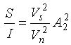
In the line below Equation 10.16 change, "which is A2 times higher" to,
"which is A22 times higher".
References:Page I-1, Answer to Problem 1.9.
The definition of signal-to-noise ratio as a power ratio (not a voltage ratio) can be found in most handbooks of electrical engineering and also in. . .
B.P. Lathi, Linear Systems and Signals, 2nd ed. Oxford, 2005, p70.
Pallas-Areny and Webster, Analog Signal Processing, Wiley-Interscience, 1999, page 16 and pages 525-526.
Millman and Halkias, Integrated Electronics: Analog and Digital Circuits and Systems, McGraw Hill, 1972, p403.
Horowitz and Hill, The Art of Electronics, 2nd edition, Cambridge, 1989, p434.
Hambley, Electronics: A Top-Down Approach to Computer-Aided Circuit Design, Macmillan, 1994, p382.
The definition of signal-to-interferance ratio as a power ratio and as a special case of a signal-to-noise ratio can be found in the Wikipedia article "Signal-to-interference ratio."
A discussion of Signal to Noise ratio as a power ratio can be found in the Wikipedia article , "Signal-to-noise ratio."
A few other authors along with Sedra and Smith treat signal-to-noise ratio (or signal to interferance ratio) as a voltage ratio (not a power ratio), nevertheless, it does not agree with industry practice. Some examples are:
Gray and Searle, Electronic Principles: Physics, Models, and Circuits, Wiley, 1969, p622. (This is the earliest published book Prof. De Boer could find with this error in it.)
Donald Neamen, Microelectronics Circuit Analysis and Design, 4th ed., McGraw Hill, 2010, p859.
Change the second instance of "157" to "106". Also fix the grammar: Just before the first instance of "a 157" add the word "with".
Page I-2, Answer to Problem 4.2 parts a and d
Some negative signs are missing from the textbook.
The answer for part (a) should be "5.00 V; 1 mA."
The answer for part (d) should be "5.00 V; 0 mA."
(Posted 9/16/2010)
Page I-2, Answer to Problem 4.9 part b
The answer should be "1.00 V; 0 mA."
Page I-2, Answer to Problem 4.10
Correct answers are (a) 3.0 V; 0.15 mA (b) 0.5 V; 0 A
Page I-2, Answer to Problem 4.18
Change "0.345V" to "173 mV" (Contributed by Alice, Posted 9/22/2010)
Page I-2, Answer to Problem 4.68
Delete "0.13;" (Posted 9/28/2010)
Page I-2, Answer to Problem 4.70.
Change "94.8%" to "47.4%."
(Alternatively, change the question. Specifically change, "For what fraction of a cycle does each diode conduct?" to, "For what fraction of a cycle is there conduction through the load?" Answer: 94.7%)Page I-2, Answer to Problem 5.59 (b) is inaccurate.
Change "4.6 μA" "to 4.5 μA". Students should express answers to part (b) that are accurate to at least 3 significant figuresone more than given in this answer key. Also see errata on the problem statement for 5.59.
Page I-2, Answer to Problem D5.108 Part (b) is wrong.
The correct answer for part b is 0.199 mA.
(Increasing RD cannot increase the current!)
Also see errata on the problem statement for D5.108.
Page I-2, Answer to Problem 6.1.
Some of the given answers are incorrect, and there are too many answers. The correct answers are:
6.1 active; saturaton; active; saturation; active; cutoff.
(This erratum has been corrected in later printings.)
(Posted 12/04/2012, updated 1/25/2103)
Page I-3, Answer to Problem 6.8.
Change "53.3; 0.982" to "60; 0.984"
(This erratum has been corrected in later printings.)
(Posted 12/04/2012, updated 1/25/2013)
Page I-3, Answer to Problem 6.12.
Change "3 to 15 mA; 3.05 to 15.05 mA, 135 mW"
to "1.2 mA to 6.0 mA; 1.22 mA to 6.02 mA; 54 mW"
(This erratum has been corrected in later printings.)
(Posted 1/19/2011, updated 1/25/2103)
Page I-3, Answer to Problem 6.28 part (d)
Change "0.35 V" to "4.475 V"
Also note that not all answers to this problem are given here. The authors' intent was only to give "selected" answers.
(This erratum has been corrected in later printings.)
(Updated 12/04/2012, 1/25/2013)
Page I-3, Answers to Problems in Chapter 6 numbered 6.43 and up.
If your textbook shows an answer to problem 6.70, you have an early printing of the textbook. In this case, delete the answer to Problem 6.70. (This was problem 5.54 in the fifth edition, but it is now deleted from this edition of the textbook.)
After making the above change, in the list of answers on page I-3, change problem number 6.43 (in blue type) to 6.44. Similarly, add one to all the remaining Chapter 6 problem numbers except change 6.152 to 6.154. Also note that the list is not in numeric order. A corrected list in proper order to replace the Chapter 6 answers (in the first printing at least) is shown here:
6.1 active; saturation; active; saturation; active; cutoff 6.7 0.907 mA; 0.587 V 6.8 60; 0.982
6.10 0.5; 0.667; 0.909; 0.952; 0.991; 0.995; 0.999; 0.995 6.12 1.2 to 6.0 mA; 1.22 to 6.02 mA
54 mW 6.17 0.718 V; 4.06 V; 0.03 mA 6.22 2 V; 0.82 mA; 0.57 V 6.24 0.91 mA;
9.09 mA; 0.803 V; 9.99 mA 6.28 (a) 1 mA; (b) 2 V; (c) 1 mA: 1 V: (d) 0.965 mA;
4.475 V 6.38 0.74 V; 0.54 V 6.40 3.35 μA 6.44 33.3 kΩ; 100 V; 3.3 kΩ 6.46 1.72 mA;
6 V; 34 V; 20 kΩ 6.48 150; 125; 1.474 mA 6.52 (a) 0.8 V, 2.2 V; (b) 0.3 V, 2.7 V; (c) 0 V,
3 V 6.55 0.7 V; +4.7 V; 0.5 V; (1 V; +5 V); +2.6 V (1.9 V, 2.6 V) 6.57 0.3 V; 15 μA; 0.8 ma; 0.785 mA; 1.075 V; 52.3; 0.98 6.62 (a) 0.7 V, 1.4 V; (b) 1.33 V, 1.05 mA;
(c) 0.7 V, 0 V, 1.33 V; (d) 1.4 V, 0.53 V; (e) 0.73 V, 1.43 V, 0.58 V 6.65 1.40 kΩ; the
transistor saturates. 6.71 160 V/V; 0.7 V; 4.38 mV 6.76 80 V/V 6.79 3 mA;
120 V/V; 0.66 V; 0.6 V; 0.54 V; 0.6 V 6.95 0.9 V; 20 mA/V; 164 V/V 6.103 135;
41.8 Ω; 23 mA/V; 1.09 kΩ; 0.76 V/V 6.106 8.6 kΩ; 7.7 kΩ; 77.2 V/V 6.107 0.5 mA;
0.996 V/V; 0.904 V/V 6.154 (a) 1.73 mA, 68.5 mA/V, 14.5 Ω, 1.46 kΩ; (b) 148.2 kΩ,
0.93 V/V; (c) 18.21 kΩ 0.64 V/V
The answers in the list above are not the answers that were intended to be revealed by the authors of the textbook, but many students have them in their textbooks--you may as well see them too. The answers the authors intended to print for problems numbered 6.43 and up are as follows:
6.43 0.1 mA; 10 A; 0.99 mA; 0.11 mA; 8.16 V; 21.8 mV; 6.5 V 6.45 150 kΩ; 1.5 MΩ
6.51 2.8 V; 9.33 mA; 9.3 kΩ 6.56 0.74 mA; 2.26 V 6.61 2.86 V; 2.16 V; 2.86 V
6.64 198 kΩ; 12 kΩ; 10 kΩ; 0.9004 mA to 1.07 mA; 6.17 to 4.37 V 6.76 80 V/V
6.78 100 V/V; 100 V/V; 6.95 0.9 V; 20 mA/V; 164 V/V 6.102 1000 V/V;
10,000 V/V 6.106 8.6 kΩ; 7.7 kΩ; 77.2 V/V 6.107 0.5 mA; 0.986 V/V; 0.904 V/V
6.154 (a) 1.71 mA; 68.5 mA/V; 14.5; 1.46 kΩ (b) 120 kΩ; 0.92 V/V (c) 18.21 kΩ; 0.64 V/V
The above answers appear in later printings of the textbook. If you happen to have an earlier printing, here is the list of answers your peers with newer textbooks have. The above list includes corrections of some errata that reamin in the newer printings.
(posted 1/22/2011, updated 1/25/2013)
Page I-3, Answer to Problem 6.71 (possibly erroneously labeled 6.70)
If your textbook shows "6.70 360 V/V; 0.7 V, 2 mV"
change it to "6.71 160 V/V; 0.7 V, 4.38 mV"
Otherwise, insert this answer which is entierly missing in some printings.
(posted 1/25/2013)
Page I-3, Answer to Problem 6.76 (erroneously labeled 6.75)
If your textbook shows "6.75 100 V/V"
change it to "6.76 80 V/V"
(This erratum has been corrected in later printings.)
(posted 1/22/2011, updated 1/25/2013)
Page I-3, Answer to Problem 6.52 (possibly erroneously labeled 6.51)
If your textbook shows
"6.51 (a) 1.3 V, 3.7 V; (b) 0.3 V, 4.7 V; (c) 0 V, +5 V"
change it to
"6.52 (a) 0.8 V, 2.2 V; (b) 0.3 V, 2.7 V; (c) 0 V, 3.0 V"
Otherwise, insert this answer. (It is entierly missing from some printings.) (posted 1/22/2011, updated 1/25/2013)
Page I-3, Answer to Problem 6.62 (possibly erroneously labeled 6.61)
If your textbook shows
"6.61 (a) 0.7 V, 1.8 V; (b) 1.872 V, 1.955 mA; (c) 0.7 V, 0 V, 1.872 V;
(d) 1.9 V, 0.209 V; (e) 1.224 V, 1.924 V, 0.246 V;
change it to
"6.62 (a) 0.7 V, 1.4 V; (b) 1.33 V, 1.05 mA; (c) 0.7 V, 0 V, 1.33 V;
(d) 1.4 V, 0.53 V; (e) 0.73 V, 1.43 V, 0.58 V;
Otherwise insert this answer. (It is entirely missing from some printings.)
(posted 1/22/2011, updated 1/25/2013)
Page I-3, Answer to Problem 6.64
If your textbook shows "6.64 1.08 kΩ; the transistor saturates"
then add (in the margin in front of the existing "6.64") "6.64 198 kΩ; 12 kΩ; 10 kΩ; 0.9004 mA to 1.07 mA" and also skip to the next item in this errata list and perform that correction too because your textbook is an early printing with different errata compared to later printings.
Otherwise, Change "164 k; 13 k; 10 k; 0.865 mA to 1.01 mA;"
to "198 kΩ; 12 kΩ; 10 kΩ; 0.9004 mA to 1.07 mA"
(posted 1/25/2013)
Page I-3, Answer to Problem 6.65 (possibly erroneously labeled 6.64)
If your textbook shows "6.64 1.08 kΩ; the transistor saturates."
change it to "6.65 1.40 kΩ; the transistor saturates."
Otherwise insert this answer. (It is entierly missing from some printings.)
Also note the clarification of the problem statement.
(posted 1/22/2011, updated 1/17/2013, 1/25/2013)
Page I-3, Answer to Problem 6.95 (possibly erroneously labeled 6.94)
If your textbook shows "6.94 1.25 V, 20 mA/V, 150 V/V"
Or, if your textbook shows "6.95 1.25 V, 20 mA/V, 150 V/V"
change it to "6.95 0.9 V, 20 mA/V, 164 V/V"
(posted 1/22/2011, updated 1/25/2013)
Page I-3, Answer to Problem 6.106 (possibly erroneously labeled 6.105)
If your textbook shows "6.105 9.3 kΩ, 28.6 kΩ, 143 V/V"
change it to "6.106 8.6 kΩ, 7.7 kΩ, 77.2 V/V"
Otherwise insert this answer. (It is entierly missing from some printings.)
(posted 1/22/2011, updated 1/25/2013)
Page I-3, Answer to Problem 6.107 (possibly erroneously labeled 6.106)
If your textbook shows "6.106 1 mA, 0.996 V/V, 0.63 V/V"
or if it shows "6.107 1 mA, 0.996 V/V, 0.63 V/V"
change it to "6.107 0.5 mA, 0.986 V/V, 0.904 V/V"
(posted 1/22/2011, updated 1/25/2013)
Page I-3, Answer to Problem 7.15
Change "1.4 V2" to "1.07 V." (posted 02/05/2011)
Page I-3, Answer to Problem D8-11
Answers to the quesitons, "What is the differential voltage, vid = vG1 vG2, for which the ratio of drain currents iD2/iD1 is 1.0? 0.5? 0.9? 0.99?" are not given.
Also note errata on the problem statement for 8.11.
Page I-3, Answer to Problem D8.38
Change "(I/2)" to "(αI/2)" in each instance of parts a and b.
In part c change "4 V" to "4.04 V"
In part d change "0.4 mA, 10 k
" to 0.404 mA, "10 k." Also note errata on problem D8.38
Page I-3, Answer to Problem *8.118
Change "(a) 0.97 mA; (b) 2.23 kΩ, 129 Ω; (c) 2.86 × 10⁴ V/V"
to "(a) 1.0 mA; (b) 2.32 kΩ, 128 Ω; (c) 2.90 × 10⁴ V/V"
(posted 5/02/2013)
Page I-4, Answer to Problem 9.66
Change "139 V/V; 21.21 GHz; 1.99 MHz; 83.22 MHz; 1.99 MHz;
to "139 V/V; 21.2 GHz; 2.27 MHz; 86.3 MHz; 2.27 MHz;
(posted 5/02/2013)
Additional notes: (Clarifications--not errata)
Page 45 Problem 1.24
An equivalent problem (Implying the same questions and giving the same answer) is as follows:
Suppose a temperature sensor is at a temperature of T degrees centigrade. At this temperature and without the load resistance connected, an ideal voltmeter shows the output voltage to be V millivolts. A 10 kΩ load resistance is now connected but the temperature is not changed. The terminal voltage of the sensor is reduced to V 10 millivolts. Now the temperature is increased until the terminal voltage returns to V millivolts. It is observed that the temperature was increased 10 degrees centigrade to accomplish this. Now the load is disconnected but the temperature is held constant at the elevated amount of T + 10 degrees centigrade. The output of the sensor is now V + 20 millivolts. What is the source resistance of the sensor?
(Posted 9/06/2012)
Page 112 Problem D2.34 part (b)
The output resistance of the "current amplifier" is requested. The variable vo designates the output of the "operational amplifier" which is confusingly, not the output of the "current amplifier." The output of the "current amplifier" is found at the two terminals of RL.
Add label VL under RL and polarity marks "+" and "" on either side with the "+" on the left. Then the output of the "current amplifier" is at the two terminals marked by these new polarity marks. Resistor RL is the load on the "current amplifier."
To find the output resistance of the "current amplifier," replace RL by a test source, Vx such that VL = Vx. Then, with the input of the "current amplifier" zeroed (iI = 0 or open) find iL in terms of VL. Then the output resistance is Ro = VL/iL. See text page 27 for the basic theory. Note that for a current amplifier, a zero input is an open. (Whereas, for a voltage amplifier a zero input is a connection to ground.)
Page 118. Problem *2.77 and Figure P2.77
The two resistors connected to the non-inverting ("+") inputs of the op-amps are not the optimal values. For this circuit, the non-inverting input of the top op-amp should be connected to node A through a 6.67 k
resistor. The
non-inverting input of the bottom op-amp should be connected to
ground through a 7.5 k resistor.
The assumption of an "ideal" op-amp makes these resistors
unimportant to the operation of the circuit, no matter what their
values are. If the op-amps are not ideal, these two resistors
reduce the effect of input bias currents. If this makes no sense
to you and you are further interested, ask professor De Boer about
it.
Page 120. Problem D**2.93
For stylistic consistency, in the denominator of the equation the second instance of j could be inside the parenthesis. The complete denominator is then
[1 + (ω1/jω)][1 + (jω/ω2)]
Either way, the equation means the same thing.Page 192 Example 4.7
In the statement of the example problem VZ = 6.8 V at IZ = 5 mA is given. This does not mean that the actual diode current, labeled in blue as "IZ" on the figure, is necessarily 5 mA. It only means that if IZ is 5 mA then VZ will be 6.8 V.
(In the figure, in both parts (a) and (b), VO = VZ.
Page 226 Problem 4.76
Here is the question stated in one piece, with errata corrected:
4.76 Let the full-wave rectifier circuit shown in Figure 4.22 (page 198) operate from a 120 V (rms) 60 Hz residential supply line. Let the transformer have a 5:1 (step down) turns ratio. (For each half of the secondary then the turns ratio is 10:1.) Let the diodes be silicon diodes that can be modeled to have a 0.7 V drop for any forward current. Let the load resistor be 1 kΩ. Augment this rectifier circuit with a capacitor chosen to provide peak-to-peak ripple voltage of
(i) 10% of the peak output and
(ii) 1% of the peak output. In each case:
a.) What average output voltage results?
b.) For what fraction of a cycle is there conduction through the rectifier?
c.) What is the average current through each diode during conduction?
d.) What is the peak current through each diode?
Note: a "rectifier" is a diode orin this casea set of diodes used to convert alternating current to direct current.
Also see above for errata on this problem.
(The original problem statement refers to problem 4.69 and 4.75. Problem 4.75 refers to Problem 4.68. Problem 4.68 refers by name (not by figure number) to Figure 4.21, but students are supposed to substitute figure 4.22 because problem 4.69 refers to that by name and by way of superceding problem 4.68. Students have a hard time understanding the question!) (updated 10/21/2010)
Page 226 Problem 4.77
Here is the question stated in one piece, with errata corrected:
4.77 Let the bridge rectifier circuit shown in Figure 4.23 (page 199) operate from a 120 V (rms) 60 Hz residential supply line. Let the transformer have a 10:1 (step down) turns ratio. Let the diodes be silicon diodes that can be modeled to have a 0.7 V drop for any forward current. Let the load resistor be 1 kΩ. Augment this rectifier circuit with a capacitor chosen to provide peak-to-peak ripple voltage of
(i) 10% of the peak output and
(ii) 1% of the peak output. In each case:
a.) What average output voltage results?
b.) For what fraction of a cycle is there conduction through the secondary
winding of the transformer?
c.) What is the average current through each diode during conduction?
d.) What is the peak current through each diode?
Also see above for errata on this problem.
(The original problem statement refers to problem 4.70 and 4.75. Problem 4.75 refers to Problem 4.68. Problem 4.68 refers by name (not by figure number) to Figure 4.21, but students are supposed to substitute figure 4.23 because problem 4.70 refers to that by name and by way of superceding problem 4.68. Students have a hard time understanding the question!) (updated 10/21/2010)
Page 346, Problem 5.114.
The "50-
coaxial cable" is
just a wire with a shield around it. Specifically, the
resistance from one end of the cable to the other is ZERO.
The reisistance from the drain of Q1 to
the source of Q2 is 0 . However, the cable is long enough so that it takes a noticable amount of time for a signal to travel through the cable (or wire). Because of this propagation time, the cable works better when the load on the cable is of the specific value for which the cable is designed. This cable is designed for a 50
load, thus it is called
a "50 cable," but just as
for a wire, the resistance of the cable from end-to-end is
(practically) zero. Thus the goal of the problem is to make
Ri2, the resistance looking into the source
of Q2, be 50 so that the cable works as well as possible with
respect to transferring high-bandwidth (fast) signals.Also see errata on problem *5.114.
Page 347, Problem 5.117.
This problem makes reference to Figure 5.60(a) (page 321) and Exercise 5.41 (page 322). Exercise 5.41 refers to Figure E5.37 (page 315.) Figure 5.37 cannot be understood apart from Exercise 5.37 (also on page 315.) Asking students to ferret through all this just to gain given information for the problem is a waste of their time. Here is the problem restated with all the given information included.
*5.117 In this problem we investigate the large-signal operation of the source follower of Fig. 5.60(a). Specifically, consider the situation when negative input signals are applied. Let the negative signal voltage at the output be V. The current in RL will flow away from ground and will have a value of V/RL. This current will subtract from the bias current I, resulting in a transistor source (and drain) current of (I V/RL). One can use this current value to determine vGS. Now, the signal at the transistor source terminal will be
vo = V superimposed on the dc bias voltage, which is VGS (corresponding to a drain current of I). We can thus find the signal voltage at the gate, vi. In Figure 5.60(a), let I = 0.5 mA, k'n(W/L) = 1 mA/V2, RL = 15 kΩ and ignore the Early effect. Note that this bias situation is similar to that used in Exercises 5.37 on page 315 and Excercise 5.41 on apge 321. For this circuit, find vi if vo = 1. Repeat for vo = 5, vo = 6, and vo = 7. At each output voltage, find the large signal gain, vo/vi and compare to the small signal value, Av found in Excercise 5.41 (page 322). What is the largest possible negative-output signal?
(Posted 12/04/2012)
Page 473, Problem D6.65.
The problem should be re-worded as follows:
D 6.65 Consider the pnp transistor in the circuit of Fig. P6.65.
a.) If the transistor has β = 50, find the value for RC to obtain VC = +3 V.
b.) Using the value for RC found in part (a), what happens if the
transistor is replaced with one having β = 100?
Also note the errata on the answer in the back of the book.
(The problem as stated in the textbook leads most students to simply repeat part (a) with
β = 100 to find a new value for RC. This is not the author's intent nor is it an interesting problem.) (Posted 1/20/2011)
Page 584, Problem 7.95.
For the BJT transistor assume
is infinite. For both the MOSFET and the BJT
ignore the Early effect.
Pages 826, 828, Figures 10.14, and 10.15.
In parts b and c of Figure 10.14, the circuit element h22 has units of conductance (siemens). The actual resistance is (1/h22)
. In part (c) of Figure 1.14
h22 is shown in parallel with
RL. Then in Figure 10.15 this same
conductance is shown instead as a resistance,
R22. This is not a miss-print since
conductors and resistors share the same symbol. It is
just a matter of notation. Remember that
R22 = 1/h22.
Disclaimer: This list of errata is provided by Professor De Boer for the use of his students in his courses. Professor De Boer has no connection to the book's publisher or the authors of the textbook. This list is offered as is, with no guarantee of any kind. It is likely to be incomplete at the least.