This article discusses how to interface devices to computers and microcontrollers
Many hobbyists have a fear of computers when they first start out tinkering with electronics. Computers are mysterious black boxes whose inner workings are beyond understanding, or so they think. In reality, computers aren't all that complicated.
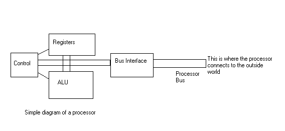
The heart of a computer is the processor. This is the little guy who does all
of the thinking, so to speak. While processor designs vary greatly, they all do
generally the same things. Let's consider a fairly simple computer, similar to
what you find in older CISC (Complex Instruction Set Computer) type machines.
Registers are just a bunch of flip-flop circuits arranged in organized groups (generally in some multiple of 8).
The Arithmetic Logic Unit (ALU) is the guy who does all of the real work, as far as the number crunching is concerned. This is a circuit that can do things like add, subtract, multiply, divide, and do logic functions like and, or, not, exclusive or, etc. Generally speaking, an ALU can only take two numbers as its input, and produce a third number based on one of these arithmetic or logic functions.
The control circuitry is what makes it all work. The control circuit in a simple processor like this is generally just a finite state machine, and the simplest finite state machine is just a rom. The code in the rom is sometimes referred to as the microcode.
The way this whole thing works is that the processor goes through various states. In each state it does something different.
In the instruction fetch stage places the value of one of its registers called the program counter onto the bus and sets the control lines to do a read operation. This causes the processor to read a number from a memory that is external to the processor. This number is then stored in a temporary register. Each number corresponds to a different opcode in the processor. One opcode might be for ADD, another might be for SUBTRACT, a third might be to call a subroutine, and so on.
The next step is to decode the instruction. A typical instruction might be "Add the number at memory location 4100 to register A" (in digital form this might be a byte to specify the ADD instruction, a second byte to specify register A, and two more bytes to store the number 4100). The ALU can add two numbers, but we only have register A inside the cpu. So, we have to do another memory access to get the number at location 4100.
Now that we have both numbers inside the processor, we just put them on the inputs of the ALU and set its control lines for ADD. Voila! Now we have our answer.
The problem is that our answer is just sitting in a temporary register. So, if we don't do anything with it, it's going to go to the great big bit bucket in the sky. The last thing the processor does is store the answer somewhere. In the case of our add instruction, we put the result back into register A inside the cpu. A different type of instruction might write the result to a memory location outside of the cpu.
Ok, we're done. Now the processor goes back to the instruction fetch stage, and starts the whole thing all over again.
This type of architecture is generally called CISC (complex instruction set computer) because the way you make the computer "better" is to make it do more types of instructions. For example, the 8085 and 6502 processors, which follow this type of architecture, couldn't even multiply. The 8086 was "better" because it could multiply and divide, and a whole bunch of other things that the older processors couldn't do.
As computers evolved, people started making seperate pieces of hardware to do each of the various things that the processor needed to do, so that overall the computer could be faster. For example, you could have a piece of hardware that only fetched instructions, and did nothing else. Then you could have another piece of hardware that only decoded the instruction, and a third piece that only did the execute, and so on. This makes things a whole lot faster, since the processor can execute one instruction while fetching another and decoding a third, etc. but it also adds drastically to the complexity of the processor. This idea is called "pipelining", since the instructions follow a "pipe" through the processor as they move from one stage to the next. In order to make the whole thing work, people generally strip down the processor to only the most essential instructions, which requires less hardware to impliment. Hence these are generally called reduced instruction set computers, or RISC.
Of course, in the real world, it gets a lot more complicated. A pentium is basically a CISC computer built around a RISC type pipeline (in fact, it's a dual pipeline - under certain circumstances a pentium can execute two instructions at once) with a floating point coprocessor, which is also pipelined, tacked on to the end of the architecture. It's quite messy, architecturally speaking.
So, now we know basically what our processor is doing. It's constantly fetching instructions, then fetching the data it needs for those instructions, executing, and storing the answer either inside the cpu or back out in the memory. The processor connects to the outside world via the processor's bus. A bus is just a big collection of signals all shoved together, generally interconnecting to a bunch of different devices all in parallel. Bus signals come in three groups: Address, Data, and Control. Data is transferred either from the processor to some peripheral device, or from the peripheral to the processor (actually, just to make it more complicated, some computers allow peripherals to take control of the bus and transfer data from one peripheral device to another without involving the cpu).
The data transfers occur in very precisely defined bus cycles. Generally speaking, the processor places the address desired onto the address portion of the bus. This could be the address from the program counter in the case of an instruction fetch, or it could be the address of an operand from the address decode, or it might be a destination address from the writeback section. We don't know. All we know is that it is a bus access cycle. The processor also tells us what type of bus cycle it is, using the control lines. There might be one line for a memory read and another for a memory write, a third for an I/O device read and a fourth for an I/O device write. If it's a write operation, the processor will put the data to be written on the data bus. If it's a read operation, the processor expects the peripheral device to put the data on the data bus. At the end of the bus cycle, the processor will either read the data from the data bus (if it's a read cycle) or will just finish the bus cycle (if it's a write). Then the next bus cycle begins.
We can get our read and write signals directly from the control portion of the bus.
Hey, that's it! Simple enough, eh? If the processor does a read at location 4096, our address decoder will put out a chip select signal and the read command line from the bus will be active. This tells our chip that it's selected and it's a read operation, so our register puts its data onto the bus. Eventually, the processor reads the data, but our chip doesn't know when. All our chip knows is that the chip select and the read signals eventually go away, so it releases control of the data bus at this point.
The process is similar for a write operation. When our register chip detects the write and the chip select, it latches the data from the data bus into the chip. The processor doesn't know exactly when this happens, all it knows is that it leaves the data on the data bus for one bus cycle and hopes that whoever is out there does what they are supposed to with it. At the end of the bus cycle, the command lines go away and the chip is no longer selected.
In our imaginary computer, everything's all nice and neatly organized. There are seperate address and data lines, and everyone is happy. Unfortunately, the real world is not so nice. If you are designing a real processor, you look at the DIP package that perhaps has been allocated for this procssor, and you start adding up the signals you need. For example, an 8086 needs 20 address lines, 16 data lines, and a whole bunch of control lines. Ack! That's a lot of pins! Let's see... 20 plus 16 is 36, plus power and ground is 38, and now we've got to add how many control lines? There's no way in heck this will fit into a 40 pin DIP package!
The solution to this problem is to multiplex your bus. This means you put the address and data lines all on the same pins. The first 16 pins are both address and data, and then (since there aren't 20 data pins) the last four are only for the address. Of course, you do need a control line to tell you when the pins have the address and when they have data, but that's one additional control line added while 16 data lines have just disappeared, for a net savings of 15 pins!
So, the processor designer is all happy, the manufacturing folks are all happy, it seems like everyone is happy, except for us. Why? because our job just became more difficult. We can't just build a simple address decoder. Our circuit is going to get confused once the address disappears from the bus and data is placed on those lines. We have to latch the address into temporary registers, so that we have valid address lines throughout the entire bus cycle. Once we add some address latches, we're back to using our simple address decoder, and we're back in business!
Okay, enough theory. Let's see some real stuff!
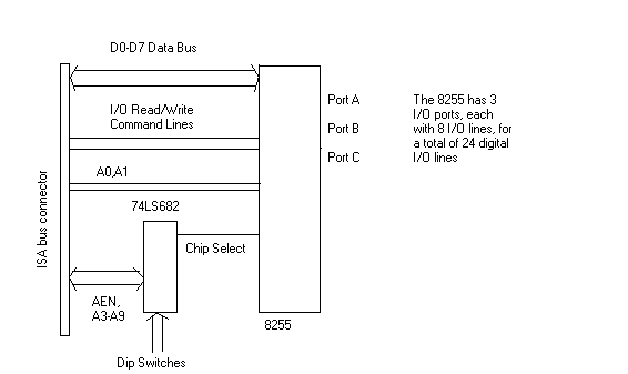 Here's a
really, really simple ISA card. The ISA bus has some nice features. For example,
the folks at IBM already put the address latches on the motherboard so you don't
have to use your own. There are seperate address and data lines already on the
bus. This example uses an 8255 chip, which also has some nice features, namely
that it decodes the command lines and two of the address lines for you. The way
this works is that the 74LS682 (an 8 bit compare chip) compares the address on
the address bus with the binary value set by the dip switches. If the numbers
match, the chip select for the 8255 is activated. The 8255 can tell from A0 and
A1 which port inside the 8255 is being accessed, and it also can tell what type
of operation it is from the I/O command lines (read or write).
Here's a
really, really simple ISA card. The ISA bus has some nice features. For example,
the folks at IBM already put the address latches on the motherboard so you don't
have to use your own. There are seperate address and data lines already on the
bus. This example uses an 8255 chip, which also has some nice features, namely
that it decodes the command lines and two of the address lines for you. The way
this works is that the 74LS682 (an 8 bit compare chip) compares the address on
the address bus with the binary value set by the dip switches. If the numbers
match, the chip select for the 8255 is activated. The 8255 can tell from A0 and
A1 which port inside the 8255 is being accessed, and it also can tell what type
of operation it is from the I/O command lines (read or write).
This is not an example of a "perfect" ISA card. If you look closely, you'll notice that we're only decoding a total of 9 address lines, out of 16 available. This means that our card will respond to addresses that it was not intended for. Historically, many cards on the ISA bus only decode the first 10 address lines, so this really isn't much of a problem for all of the addresses that are above 0x3FF. Because the A2 bit isn't decoded, the four ports on our 8255 will be repeated. In other words, the four ports of the 8255 will show up as designed at BASE+0, BASE+1, BASE+2, and BASE+3, respectively (where BASE is the base address we select via the dip switches), but they will show up again at BASE+4, BASE+5, BASE+6, and BASE+7, which is not necessarily what we wanted them to do. If we used a more complicated address decoder that used more bits, then we would not see the second reflection of the I/O ports in our memory map.
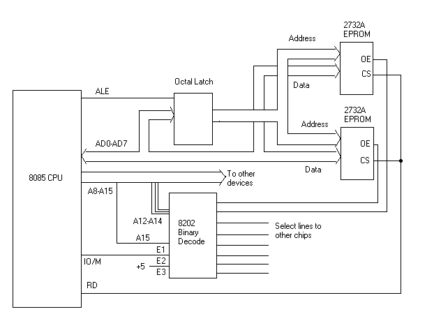 Here's
another example. This shows how to connect two EPROM chips to an 8085 CPU. The
8085 is an older 8 bit cpu. It has 64k of address space, which means it has 16
address lines, and 8 data lines. The 8 data lines are multiplexed with the lower
8 address lines.
Here's
another example. This shows how to connect two EPROM chips to an 8085 CPU. The
8085 is an older 8 bit cpu. It has 64k of address space, which means it has 16
address lines, and 8 data lines. The 8 data lines are multiplexed with the lower
8 address lines.
The first thing we need to do is latch the address/data lines to create a seperate address bus. This is done with a simple octal latch, which is driven from the Address Latch Enable (ALE) signal from the cpu. There are several different chips you can use as a latch, such as the Intel 8212 or the 74LS373. When ALE goes high, the address is valid on the address/data bus, so that's when we latch it into our register. For the rest of the bus cycle, the address will be valid on our seperate address bus that we created. The upper half of the address bus from the cpu, lines A8 to A15, are not multiplexed, so we don't need to latch them.
Now we have a seperate address and data bus, so we can connect these signals to our EPROM chips. A 2732 EPROM is a 4k by 8, meaning it has 4k worth of 8 bit bytes. We can connect address lines A0 to A11 to the EPROMs, which will select the desired address that we want to read out of the chips.
Next we have to come up with some sort of select logic, otherwise the EPROMs will be attempting to put data on the bus all the time, which would interfere with other chips in the system. We need to decode the upper address lines, A12 through A15. When they are all zero, then we want to select our lower address EPROM, and when A12 is high but all of the others are low, then we want our upper address EPROM. This will map our EPROMs into memory locations 0000H to 0FFFH for the lower EPROM and 1000H to 1FFFH for the upper EPROM. We definately need the lower EPROM to be at 0000H to 0FFFH, since the reset vector for the 8085 is in this address space, but our second EPROM could really be anywhere we desire. It's just easier from a programming standpoint to have them both contiguous in memory, so we can treat them as one big 8K ROM.
There are several ways we could make our address decoder. We could create a truth table and simplify it down to basic logic gates, and construct the circuit from these. We could use a ROM of some sort, which would have the truth table coded inside of it. Using a ROM is a good idea for development systems because you can easily re-map all of your chips in the system just by changing the code in the ROM, which is much easier than rewiring much of the select logic on the board.
In this case, we are going to use an Intel 8205 chip for our address decoder. The 8205 chip will drive one of its outputs low, depending on the state of the three address lines we give it (A12 to A14). What this means is that each of the eight outputs corresponds to a 4K block of memory space. If the address is within that block of memory, then its corresponding output line will be driven low. We connect our lower address EPROM to the first output, and our higher address EPROM to the second output. We also have to connect the read command line from the CPU to our EPROMs, so that they will only be active when their address is selected and it is a read cycle from the CPU.
The 8205 has three enable lines, two of which are active low and the third is active high. If we use our highest address bit (A15) on one of the active low enables, then our chip will only be active when the address is in the lower 32k of memory space. Then we can just use A15 as an active high select line for the upper 32k of memory, which would be useful for perhaps a 32k SRAM. In this example, the second active low enable is tied to the IO/M line from the cpu, so that our chip is further restricted to only be active when it's a memory cycle on the bus, and not an I/O cycle. The active high enable on the 8205 isn't used, so we just strap it to +5.
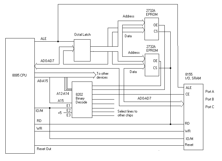
This next example shows how to add an 8155 to the above 8085 circuit. The 8155 has three parallel I/O ports and 256 bytes of static ram. It will therefore respond to both memory and I/O bus cycles. We need to connect our data lines AD0 through AD7 to the chip. The 8155 has built in latches, so we don't need to give it address signals from our latched address bus that we already created, but we do need to give it the ALE signal from the cpu. The 8155 has read and write command lines, which we just connect to the read and write command lines from the cpu. We also need to connect the IO/M signal so that the 8155 knows whether it's a memory or an I/O bus cycle. If we were using this circuit as the brain for a robot, for example, we might want to add several more 8155 chips to the circuit. They would all have the same data and control lines connected to them, and would only differ in that each would have their own select line coming from the 8205.
We have five select lines left over, which we could use for maybe a few more 8155 chips and perhaps some 8251 chips for some parallel and serial I/O lines, respectively. Combine this with the SRAM mentioned above, and you pretty much have a complete single board computer on your hands.
Most computers have built in I/O ports of some sort, so quite often you'll be interfacing to one of these ports rather than to the system bus of the processor. These I/O ports will generally be either serial or parellel ports. Serial ports are usually RS-232, which is dealt with in another article. There are also things like USB ports which due to their complexity will not be discussed here.
For this discussion, let's talk about parallel ports. Most computers have one, of some sort or another. The old Commodore 64 had one. You could buy one for the Apple II, although it did not come as standard equipment. The IBM PC has the printer port, or there's an example of an ISA interface that gives you three parallel I/O ports earlier in this article. On all of these and other systems, you are still talking about basically the same thing. You have a bunch of single bit TTL inputs and/or outputs.
TTL outputs aren't very useful unless you are interfacing to another digital
logic circuit. Otherwise, they don't have enough beef to handle an external
device. A simple solution is to use a transistor to drive the output load. 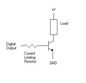
In this circuit, the value of the base resistor is not critical. It must be high enough to prevent too much current from damaging the transistor, but low enough that the transistor is still driven into saturation when the digital output is high. When the digital output is low, the transistor will be off, and no current will flow through the load. When the digital output is high, then the transistor will conduct, and current will flow through the load. Current flows from the load into the transistor, so this is called a sinking circuit, as opposed to a sourcing circuit, in which current would flow out of the circuit into the load. Transistor circuits can generally sink more current than they can source, so this is a common configuration. If you need to source current, then you can use a resistor in place of the load in the above circuit, which will produce an output that is inverted from the state of the digital output line, and you could then connect this to another transistor in a voltage follower configuration so that you would get more current drive capability.
You may have noticed that the above circuit uses +V and not +5 as the voltage source for the transistors. This type of circuit is also useful to connect devices that require a higher voltage than 5 volts to a digital output.
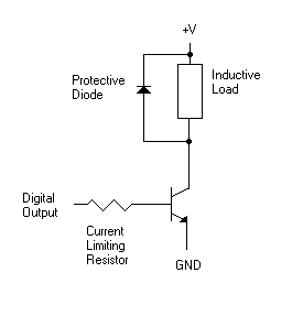
The circuit shown above is going to get you in real trouble if you use it to drive an inductive load (like a relay). What happens is that a relay is an energy storage device, and when you turn the output off, all of that energy has to go somewhere. If you don't do anything to protect your circuit, this energy can easily backfeed in through your digital output line, which can wreak all sorts of havoc on your digital system.
Fortunately, this has a simple solution. All you need to do is place a reverse biased diode across the leads of the inductor. When the circuit is on, the diode will be reverse biased and so it will not conduct current. When the circuit turns off, the energy in the inductor will go through the diode and will be disippated as heat, thus sparing your digital circuit from damage.
Optoisolators are another thing you can use to prevent damage to your system. An optoisolator is just an LED that shines onto a phototransistor. Usually they are all neatly packaged inside a single little box, but you can make your own out of discrete parts (just make sure that light can't accidentally hit your phototransistor from an outside source). When the LED is on, it shines onto the phototransistor to make it turn on. Since the connection is optical instead of electrical, any electrical noise or damaging voltage on the load side is completely isolated from your digital output. You need a resistor to limit the current into the LED (just as you would for any normal LED). On the output side, you connect your circuit the same way you would for any other transistor driven circuit.
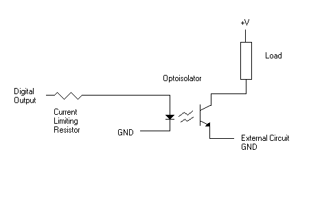
Optoisolators come in a variety of packages, some with darlington transistor pairs on the output side for greater current capability (but lower turnoff time) or schmidt triggered logic gates on the input side instead of a simple phototransitor. You can also get them with two LEDs in parallel on the input side, so that they can be used with AC inputs.
You can also use optoisolators in the reverse direction to prevent damage to inputs to your circuit.