This article covers the basics of schematic diagrams.
Schematic diagrams (often just referred to as schematics) are a way to express how parts are connected together. Symbols are used to represent each part, and lines are used to represent connections between parts. It is important to note that not all schematics use the exact same symbols or connections.
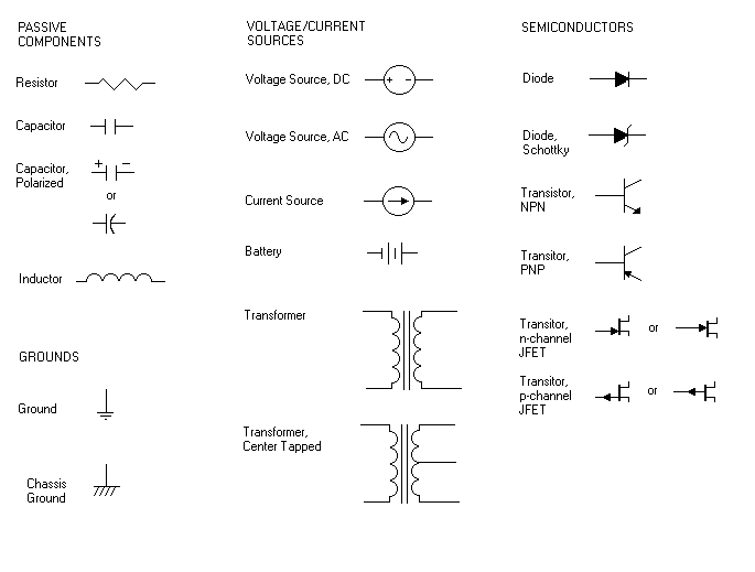
These are the symbols commonly used on schematics, and the parts that they
represent.
It is important to note that the connections shown on a schematic diagram represent ideal connections. In the real world, there is no such thing as an ideal conductor. Therefore, a schematic is an approximation of a circuit. Usually, the resistance of the wire, or the capacitance or inductance of a particular circuit path is negligable to the operation of the circuit, and can be safely ignored.
Lines are used to show connections between parts. When multiple connections exist, they are usually represented by drawing a dot where the two lines intersect. It is possible for many lines to converge to a single connection, but for clarity, most dots will only connect two lines.
When two lines intersect, but they do not have a dot drawn over the
intersection, this simply means that there is no connection between these two
circuits. Sometimes, people will go out of their way to emphasize that there is
no connection, by drawing a small "hump" over the first line to show that the
second line is above it, and not touching it. This is not necessary, and either
method is acceptable. 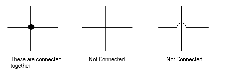
An important concept in electronics is that of a "node". A node is simply a point where two or more parts are connected. The confusing part about a node is that the lines do not represent wires. They simply represent a connection. A very long line does not imply a very long wire, nor does a short line imply a short wire.
In the following circuit, there are 3 nodes, labled A, B, and C. Note that no
matter how the circuit is drawn, the same parts are always connected to the same
nodes. In other words, node A is always connected to the positive side of the 9
volt source and one side of resistor R1, node B is always connected to R1, R2,
and R3, and node C always connects R2, R3, and the negative side of the 9 volt
supply. It does not matter where the parts are drawn on the paper, and which way
they are oriented. It only matters that the lines be drawn in such a way that
the node relationships are preserved. Again, to emphasize the point, all of the
diagrams in the following figure describe the exact same circuit. 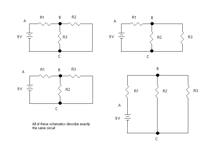
Power and ground are usually abbreviated to save space on a schematic.
Grounds (meaning signal returns) are usually shown using one of the symbols
shown above. DC power is often shown using the number and a plus or minus sign.
An arrow may be used, but many schematics will not have the arrow. The following
example shows a 5 volt DC power source connected to a resistor (the rest of the
circuit is not shown). 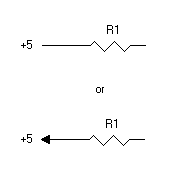
Ground is, unfortunately, a very confusing and often abused term in electronics. In circuits, we usually tie all of the signal returns together into a single voltage plane. This plane is then often connected to a physical earth ground (say, a copper rod driven into the earth) for noise reasons, etc. However, even though a connection to physical earth may not be present, it has become common in electronics to refer to signal returns as grounds. This can lead to some confusion in schematics when you see ground symbols. Often, a connection to earth ground is implied, and since it is assumed, it is not mentioned on the schematic. At other times, the ground connection only means that the signal returns are tied together, and a connection to the physical earth is not intended. It takes a little knowledge about electronics to determine what the ground symbol really means sometimes, but, unfortunately, this only comes with experience with how circuits work.
Schematics are drawn to show circuits clearly, using the fewest lines necessary (to take a famous Einstein quote out of context, "it is as complex as it needs to be, but no more"). Power and ground connections to an IC are often assumed, since the IC will not function without them. Also, if a plus and minus power supply are given, this usually means that a dual power supply with a common zero reference is present. The common reference will usually be assumed to be ground, even though no connection from the power supply to any of the ground symbols may be shown.
Often a line will dead end, and will have a signal name written above or below it. This means that the signal is continued somewhere else. For large, complex schematics, the signal may be on another page (and if they are nice, they list all signals and the pages in which they appear, but most schematic makers are not so kind). When this happens, just treat the circuit as if a line was drawn between the two points where the signal "dead ends". The tricky part is sometimes a signal will be used in a lot of places. For example, suppose we have a schematic for a computer, which has an 8 MHz clock in it. There is a circuit on one page of the schematic which shows a crystal oscillator (which generates the clock), and from here, the line simply ends with the name of the signal, SYSCLK. On the page where the cpu and its associated circuitry is shown, we again see SYSCLK, which is used as the primary clock to drive the cpu. SYSCLK also goes out across the system bus, which is shown on a seperate page, again with the name SYSCLK drawn above the line. All signals with the name SYSCLK, no matter how many times they appear on the schematic, are electrically connected together. They simply can't all be shown on the same page because the schematic is too large and complex.