This article covers some basic concepts about transistors.
If you grow some N type silicon and then grow some P type silicon on top of it, you get a silicon diode (see the article on diodes for more details). If you then grow a layer of N type silicon on top of the P type silicon, you get an NPN device. This is called a bipolar junction transistor (BJT). You could also grow some P type silicon first, and then some N type silicon, and then some P type silicon, to make a PNP transistor. NPN and PNP transistors happen to work pretty much the same way, but with opposite polarity.
You might be thinking that hey, a diode is a PN junction, and if I connected two of them back to back, then I'd have NPN, right? Well, not quite. For a lot of reasons that are difficult to explain without diving into some nasty physics, it makes a big difference whether the silicon is grown with one type right on top of another or if it's just connected by a metal conductor. So, no, you can't make a transistor out of two diodes. Sorry.
A BJT just happens to be a nifty little device that you can almost think of as an electronically controller variable resistor (hence the name TRANSISTOR). Unfortunately, BJT's are complicated little buggers, and you can very quickly get into some extremely ugly physics with things like majority and minority charge carriers, fermi levels, and equations containing enough greek letters to choke a horse. This is way too much math for your typical hobbyist, so I'll try to avoid most of the ugly stuff in this discussion.
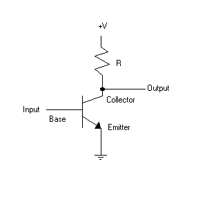
Let's start with a typical transistor circuit. This is called a common
emitter configuration, because, well, the emitter is grounded (kinda obvious,
isn't it? The emitter is connected to common, so it's a common emitter
configuration...).
The transistor has three terminals, the collector, emitter, and base. If you start out with no current flowing into the base, there will be no current flowing through the resistor. As you increase the current going into the base, eventually current starts to flow between the collector and the emitter. As the current into the base increases, so does the current flowing from the collector to the emitter, and for a very large range, you end up with a fairly linear relationship between current in the base and current from the collector to emitter. If you multiply the current in the base by some number (called the gain, or beta of the transistor) you get the current flowing from the collector to the emitter. Eventually, though, you reach a point where you put more current into the base and you don't get any more current out of the transistor.
This basically means there are three regions of operation for the transistor. The first is called cutoff, where no current is flowing from the collector to the emitter. The second region is called the forward active region. This is the big linear area. The third region, where you don't get any more current flow, is called saturation.
There are two main ways to use a transistor, either (1) an an analog device or (2) as a digital switch. If you are using it as an analog device you generally want to keep the transistor in the forward active region. If you are using it as a switch, you want the transistor to either be in saturation or cutoff (either on or off, essentially).
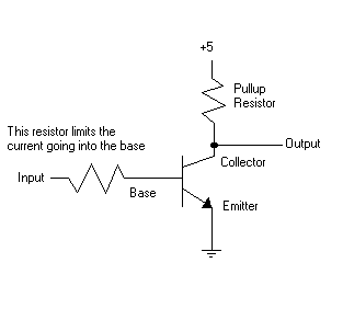 Let's add a resistor to our above
circuit, as shown. This resistor is used to limit current going into the base.
Now, let's take a look at what we've made. The transistor and the pullup
resistor make sort of a voltage divider. If the input to the circuit is a low
voltage (logic 0), then there will be no current into the base and the
transistor will be in cutoff. The transistor will therefore not have any current
flowing from the collector to the emitter, so it looks like an extremely high
impedence to the voltage divider, and hence the output of the circuit will
basically be +5 (logic 1). If we put a logic 1 (+5 volts) into the input then
the transistor will turn on, and if we've chosen our base resistor to be a small
enough value then enough current will flow to drive the transistor completely
into saturation. The transistor switches on, and since current is flowing it
looks like a very low impedence. Remember from your voltage divider equations
that this causes the output of the circuit to drop to a very low value
(essentially a logic 0).
Let's add a resistor to our above
circuit, as shown. This resistor is used to limit current going into the base.
Now, let's take a look at what we've made. The transistor and the pullup
resistor make sort of a voltage divider. If the input to the circuit is a low
voltage (logic 0), then there will be no current into the base and the
transistor will be in cutoff. The transistor will therefore not have any current
flowing from the collector to the emitter, so it looks like an extremely high
impedence to the voltage divider, and hence the output of the circuit will
basically be +5 (logic 1). If we put a logic 1 (+5 volts) into the input then
the transistor will turn on, and if we've chosen our base resistor to be a small
enough value then enough current will flow to drive the transistor completely
into saturation. The transistor switches on, and since current is flowing it
looks like a very low impedence. Remember from your voltage divider equations
that this causes the output of the circuit to drop to a very low value
(essentially a logic 0).
So, if we put a logic 0 on the input we get a logic 1 on the output, and if we put a logic 1 on the input we get a logic 0 on the output. We've just created a TTL inverter. Put six of them into an IC package and you've got a 7404 hex inverter chip.
The values of the resistors are not critical. You want the base resistor to be low enough that it drives the transistor completely into saturation but not so low that you drive too much current into the base and damage the transistor (you've got a pretty wide range between these two points). The value for the pullup resistor depends a bit on how much of a load you expect to be able to drive from the output and the saturation current for the transistor.
Let's modify our circuit again, by adding two more resistors. 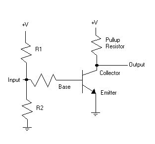 In this circuit, R1 and R2 form a voltage
divider, which feeds a certain amount of current into our transistor. We want to
chose R1 and R2 so that the transistor is right smack in the middle of its
forward active region when there is no input signal. If we've done it right, the
output of the circuit will be exactly halfway between +V and GND. As we change
the input signal, the output of the circuit will go up and down from this
midpoint, as long as we stay in the forward active region of the transistor. For
example, if we increase the input voltage, then the output voltage will decrease
as the transistor turns on a bit more and conducts a bit more between the
collector and emitter (remember, just as in the above digital circuit, we're
still sort of using the transistor in a voltage divider circuit). The important
thing is that we can get a pretty large change in output voltage for a fairly
small change in input voltage, which makes this a pretty good amplifier circuit.
In this circuit, R1 and R2 form a voltage
divider, which feeds a certain amount of current into our transistor. We want to
chose R1 and R2 so that the transistor is right smack in the middle of its
forward active region when there is no input signal. If we've done it right, the
output of the circuit will be exactly halfway between +V and GND. As we change
the input signal, the output of the circuit will go up and down from this
midpoint, as long as we stay in the forward active region of the transistor. For
example, if we increase the input voltage, then the output voltage will decrease
as the transistor turns on a bit more and conducts a bit more between the
collector and emitter (remember, just as in the above digital circuit, we're
still sort of using the transistor in a voltage divider circuit). The important
thing is that we can get a pretty large change in output voltage for a fairly
small change in input voltage, which makes this a pretty good amplifier circuit.
In the digital circuit, the resistor values weren't all that critical. This is not the case in our analog circuit. The base resistor has a large effect on the current going into the base, and since we are not driving the transistor into either cutoff or saturation, this has a large effect on the collector-emitter current, which in turn drives the output voltage of the circuit. The values of R1 and R2 are critical in finding the mid-point of the forward active region (this point is called the quiescent point, or Q-point). If our voltage divider is too low or too high, then the output will not be centered around the Q point, which reduces the amount of range that the output can swing before hitting either cutoff or saturation.
As a practical amplifier (say, for example, as an audio pre-amp), you would have to add capacitors to both the input and the output. This is because we always have a voltage on the input as a result of our R1 and R2 voltage divider (called the bias voltage, since it puts a bias on the signal going into the transistor). Similarly, when there is no signal coming into the circuit, we have a bias on the output as well (halfway between +V and ground, as mentioned above). The capacitors on the input and output will filter off the DC biases and will only pass the AC signals, which prevents the bias from this stage of the circuit from affecting other stages in our analog circuit. This type of amplifier is also not good for the final output stage of a circuit since the transistor is always on (and thus is absorbing a lot of power) even when there is no input. If you are driving a large load (like a 30 watt stereo speaker) this wastes a lot of power and generates a lot of unwanted heat.
Quite often, when you look at transistor specs you'll see one called hfe (usually written as a lower case h with the fe as a small subscript). H-parameters are just a way of modelling a device. You treat the device as a mysterious black box, and use a bunch of hybrid parameters (aka h-parameters) to describe what the mystery device does. H-parameters are really useful to us engineers, who some people say spend far too much time drawing equations with Greek letters onto sheets of paper. Actually, h-parameters are quite useful for modelling all sorts of things, not just transistors.
Hobbyists generally don't care to do a whole lot of mathematical modelling of their transistors, so I won't go into too much detail with h-parameters. Hfe, it turns out, just happens to be the current gain of the transistor (while it's in the forward active region, that is). Let's take our typical common emitter amplifier from above. All you have to do is figure out what the current is flowing in from the base to the emitter, multiply it by hfe, and voila! You have just figured out what the current is flowing from the collector to the emitter.
Beta, when used to describe a transistor, is talking about exactly the same thing, the current gain.