This article discusses semiconductors, and how they are used to make diodes (PN) and transistors (NPN and PNP).
Semiconductors are made out of silicon. You are probably already familiar with silicon, you just didn't realize it. Silicon dioxide is basically the stuff you sit on while you are at the beach. Most people call it sand. It also happens to be the stuff that glass is made out of. Yep, your front window is (probably) made out of sand. And, in case you were wondering, silicone (the stuff they used to make breast implants out of) is in fact based on silicon. So, you'll be happy to know that your computer and the Baywatch Babes both have something in common.
Sand, of course, isn't very useful for making circuits. Try it. You won't get very far. It has to be refined into a more pure form. We don't want blobs of amorphous silicon dioxide (aka unorganized sand particles). What we want are nice, neat diamond lattice crystals. The processes by which we refine silicon vary quite a bit, but basically its better to say that the crystal is grown rather than fabricated, and that its generally something that you probably don't want to be doing in your basement. There's a lot of heat and a lot of nasty materials involved.
Silicon isn't the only semiconductor used to make circuits. Germanium is also commonly used. You should note that these two elements both happen to be in the same column on the periodic table. You do remember the periodic table from chemistry class, right? See, I knew it would come in handy some day.
There are a lot of other semiconductor materials used that I won't go into much detail about. For example, Gallium Arsinide (GaAs) is often used to make LEDs, and photodetectors are often made of InSb (I'm not sure how you say that in english, but I think its Indium Antimonium - that's my guess, anwyay). Gunn diodes (used in microwaves) are usually Gallium Arsinide.
Normal silicon is called intrinsic silicon (i.e. it has no impurities or crystal lattice defects). Now that we've gone to all of this trouble to make pure silicon, the first thing we want to do is muck it all up with impurities. If we add something like Boron, Aluminum, Gallium, or Indium (once again, all from the same column in the periodic table) to either Silicon or Germanium, this creates a semiconductor with a greater concentration of holes than conduction band electrons (whew, this is getting into some ugly chemsitry, isn't it?). We call this P type silicon. If we add something like Phosphorus, Arsenic, or Antimony (which, as you might have guessed, are all in the same column on the periodic table), we get a semiconductor with more electrons than holes in the conduction band. We call this N type silicon.
The process of adding impurities to the semiconductor material is called doping.
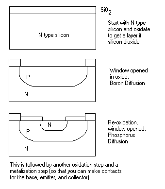
Okay, now we know how to make N and P type silicon, the first thing we want to do is make a layer of P type silicon followed by a layer of N type silicon (one method is to actually stop the growing process and change the doping material, and then restart the growing process). This creates your basic silicon diode that you are used to buying at ye ol local electronics store.
What happens if we add a third layer? Well, with three alternating layers of two materials, we have two possible choices. We can make an NPN device or a PNP device. Both of these are called bipolar junction transistors (BJT), and you can buy them as individual transistors or entire complex chips can be fabricated that use them.
If you buy a transistor (again, from ye ol local electronics shop, or perhaps
from ye ol distant electronics mailing place), it has 3 leads labeled collector,
emitter, and base. The base is the middle part (so named because the first one,
sitting on the bench at Bell Labs, was sitting on this part, if I recall
correctly). But aren't the emitter and collector the same? Well, in a sense they
are. You can reverse a BJT and it will still function as a BJT. If the device is
fabricated in such a way as to be symmetrical (like maybe growing some N
silicon, changing the doping, growing some P silicon, and changing the doping
again to grow some more N silicon) then the transistor characteristics will be
pretty much symmetrical no matter which lead you call the collector and which
one you call the emitter. However, transistors usually aren't made this way, and
you have "better" transistor characteristics in one direction than you do in the
other. This is how you can determine which lead is which if you have a
transistor that you don't have a data sheet for. Whichever configuration gives
you a better gain, etc. call the appropriate lead the collector and emitter
respectively.
The actual fabrication of these devices is a bit more complicated than what I've described, and I've only scratched the surface of some of the details involved. For example, the doping concentrations on either side of the junction affect things like the avalanche breakdown voltage, the contact potential, and the series resistance of a simple diode. The edges of the junction may be beveled or a diffuse guard ring may be used to help prevent premature breakdown across the edge of the material. Its also common to terminate the lightly doped region of a semiconductor with a more heavily doped region to ease the problem of making ohmic contact with the device.