The Basic RS NAND Latch

Direct links to other logic pages:
Combinational Logic:
[Basic Gates]
[Derived Gates]
[The XOR Function]
[Binary Addition]
[Multiplexer]
[Decoder/Demultiplexer]
Sequential Logic:
[RS NAND Latch]
[Clocked RS Latch]
[RS Flip-Flop]
[JK Flip-Flop]
[D Latch]
[Flip-Flop Symbols]
Counters:
[Basic 4-Bit Counter]
Registers:
(Coming Soon)
Return to Digital index page.
Return to Play-Hookey Home Page.
In order for a logical circuit to "remember" and retain its
logical state even after the controlling input signal(s) have been
removed, it is necessary for the circuit to include some form of feedback.
We might start with a pair of inverters, each having its input connected
to the other's output. The two outputs will always have opposite logic
levels.
The problem with this is that we don't have any additional inputs that
we can use to change the logic states if we want. We can solve this
problem by replacing the inverters with NAND or NOR gates, and using the
extra input lines to control the circuit.
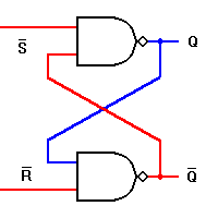
The circuit shown below is a basic NAND latch. The inputs are generally
designated "S" and "R" for "Set" and
"Reset" respectively. Because the NAND inputs must normally be
logic 1 to avoid affecting the latching action, the inputs are considered
to be inverted in this circuit.
The outputs of any single-bit latch or memory are traditionally
designated Q and Q'. In a commercial latch circuit, either or both of
these may be available for use by other circuits. In any case, the circuit
itself is:


|
|
For the NAND latch circuit, both inputs should normally be at a logic 1
level. Changing an input to a logic 0 level will force that output to a
logic 1. The same logic 1 will also be applied to the second input of the
other NAND gate, allowing that output to fall to a logic 0 level. This in
turn feeds back to the second input of the original gate, forcing its
output to remain at logic 1.
Applying another logic 0 input to the same gate will have no further
effect on this circuit. However, applying a logic 0 to the other
gate will cause the same reaction in the other direction, thus changing
the state of the latch circuit the other way.
Note that it is forbidden to have both inputs at a logic 0 level at the
same time. That state will force both outputs to a logic 1, overriding the
feedback latching action. In this condition, whichever input goes to logic
1 first will lose control, while the other input (still at logic 0)
controls the resulting state of the latch. If both inputs go to logic 1
simultaneously, the result is a "race" condition, and the final
state of the latch cannot be determined ahead of time.
|
This circuit has quite a number of limitations, and can be improved in
many ways as you'll see shortly. However, it does have a very practical
application almost without changes. Any mechanical switch experiences a
phenomenon called "contact bounce." Whenever you press the
button or change the switch position, the physical contacts will flex a
little, causing them to make and break several times before settling down.
You don't notice this when turning on a light in your home, but digital
circuits are fast enough that they do notice this behavior and
transmit it faithfully. If you are trying to test a new digital circuit by
sending it one clock pulse at a time, this will cause all sorts of
headaches.
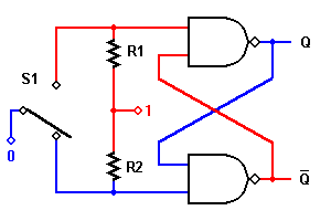
The solution is to use an SPDT (Single-Pole, Double-Throw) pushbutton
or switch, as shown in the figure to the right. Normally, the switch is of
the break-before-make type, so there will be some part of the switch
motion when all three contacts are disconnected from each other. Now, the
unconnected input is held at a logic 1 through its resistor (an electronic
component that allows an electrical connection without causing a dead
short), while the connected input is held at logic 0 by the direct
connection through the switch.
When the switch is moved to the other setting or the button is pressed,
the very first contact will cause the latch to change state, but
additional bounces will have no further effect. This eliminates the
contact bounce and sends a single, clean digital transition to the next
circuit. All of the interactive digital demonstrations behave in a
debounced fashion, and would use this type of circuit if constructed
physically.
One problem with the basic RS NAND latch is that the input levels need
to be inverted, sitting idle at logic 1, in order for the circuit to work.
It would be helpful, as well as more intuitive, if we had normal inputs
which would idle at logic 0, and go to logic 1 only to control the latch.
This much we can do simply by placing inverters at the inputs.
However, there is another problem we need to address: How to control
when the latch is allowed to change state, and when it is not.
This is necessary if we have a group of latches and want to be sure they
all change state (or not) at the same time. We'll see how both of these
concerns can be easily addressed on the next page.
Back to the Play-Hookey main page.