[Diode Logic (DL)]
[Resistor-Transistor Logic (RTL)]
[Diode-Transistor Logic (DTL)]
[Transistor-Transistor Logic (TTL)]
[Emitter-Coupled Logic (ECL)]
[CMOS]
Diode Logic makes use of the fact that the electronic device known as a diode will conduct an electrical current in one direction, but not in the other. In this manner, the diode acts as an electronic switch.
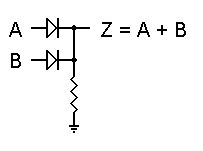
To the left you see a basic Diode Logic OR gate. We'll assume that a logic 1 is represented by +5 volts, and a logic 0 is represented by ground, or zero volts. In this figure, if both inputs are left unconnected or are both at logic 0, output Z will also be held at zero volts by the resistor, and will thus be a logic 0 as well. However, if either input is raised to +5 volts, its diode will become forward biased and will therefore conduct. This in turn will force the output up to logic 1. If both inputs are logic 1, the output will still be logic 1. Hence, this gate correctly performs a logical OR function.
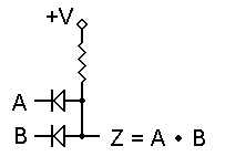
To the right is the equivalent AND gate. We use the same logic levels, but the diodes are reversed and the resistor is set to pull the output voltage up to a logic 1 state. For this example, +V = +5 volts, although other voltages can just as easily be used. Now, if both inputs are unconnected or if they are both at logic 1, output Z will be at logic 1. If either input is grounded (logic 0), that diode will conduct and will pull the output down to logic 0 as well. Both inputs must be logic 1 in order for the output to be logic 1, so this circuit performs the logical AND function.
In both of these gates, we have made the assumption that the diodes do not introduce any errors or losses into the circuit. This is not really the case; a silicon diode will experience a forward voltage drop of about 0.65v to 0.7v while conducting. But we can get around this very nicely by specifying that any voltage above +3.5 volts shall be logic 1, and any voltage below +1.5 volts shall be logic 0. It is illegal in this system for an output voltage to be between +1.5 and +3.5 volts; this is the undefined voltage region.
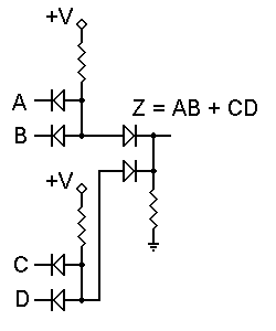
Individual gates like the two above can be used to advantage in specific circumstances. However, when DL gates are cascaded, as shown to the left, some additional problems occur. Here, we have two AND gates, whose outputs are connected to the inputs of an OR gate. Very simple and apparently reasonable.
But wait a minute! If we pull the inputs down to logic 0, sure enough the output will be held at logic 0. However, if both inputs of either AND gate are at +5 volts, what will the output voltage be? That diode in the OR gate will immediately be forward biased, and current will flow through the AND gate resistor, through the diode, and through the OR gate resistor.
If we assume that all resistors are of equal value (typically, they are), they will act as a voltage divider and equally share the +5 volt supply voltage. The OR gate diode will insert its small loss into the system, and the output voltage will be about 2.1 to 2.2 volts. If both AND gates have logic 1 inputs, the output voltage can rise to about 2.8 to 2.9 volts. Clearly, this is in the "forbidden zone," which is not supposed to be permitted.
If we go one step further and connect the outputs of two or more of these structures to another OR gate, we will have lost all control over the output voltage; there will always be a reverse-biased diode somewhere blocking the input signals and preventing the circuit from operating correctly. This is why Diode Logic is used only for single gates, and only in specific circumstances.
[Diode Logic (DL)]
[Resistor-Transistor Logic (RTL)]
[Diode-Transistor Logic (DTL)]
[Transistor-Transistor Logic (TTL)]
[Emitter-Coupled Logic (ECL)]
[CMOS]
Go to the Logic Family base page.