Resistor-Transistor Logic

Select the Logic Family you wish to examine:
[Diode Logic (DL)]
[Resistor-Transistor Logic (RTL)]
[Diode-Transistor Logic (DTL)]
[Transistor-Transistor Logic (TTL)]
[Emitter-Coupled Logic (ECL)]
[CMOS]

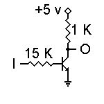
Consider the most basic transistor circuit, such as the one shown to
the left. We will only be applying one of two voltages to input I: 0 volts
(logic 0) or +5 volts (logic 1). We'll assume an ordinary NPN transistor
such as a 2N4124 -- high dc current gain, an emitter-base forward voltage
of 0.65 volt, and a collector-emitter saturation voltage no higher than
0.3 volt.
When the input voltage is zero volts (actually, anything under 0.5
volt), there is no forward bias to the emitter-base junction, and the
transistor does not conduct. Therefore no current flows through the 1K
collector resistor, and the output voltage is +5 volts. Hence, a logic 0
input results in a logic 1 output.
When the input voltage is +5 volts, the transistor's emitter-base
junction will clearly be forward biased. For those who like the
mathematics, we'll assume a similar output circuit connected to this
input. Thus, we'll have a voltage of 5 - 0.65 = 4.35 volts applied across
a series combination of a 1K output resistor and a 15K input resistor.
This gives us a base current of 4.35v / 16,000
 = 0.000271875 amperes = 0.27 ma.
Assuming a dc forward current gain of 300 for the transistor, this base
current will support a maximum of 81.5 ma collector current. However, if
we drop all but 0.3 volts across the 1K collector resistor, it will carry
4.7/1K = 4.7 ma. Therefore this transistor is indeed fully saturated; it
is turned on as hard as it can be.
= 0.000271875 amperes = 0.27 ma.
Assuming a dc forward current gain of 300 for the transistor, this base
current will support a maximum of 81.5 ma collector current. However, if
we drop all but 0.3 volts across the 1K collector resistor, it will carry
4.7/1K = 4.7 ma. Therefore this transistor is indeed fully saturated; it
is turned on as hard as it can be.
With a logic 1 input, then, this circuit produces a logic 0 output. We
have already seen that a logic 0 input will produce a logic 1 output.
Hence, this is a basic inverter circuit.
As we can see from the above calculations, the amount of current
provided to the base of the transistor is far more than is necessary to
drive the transistor into saturation. Therefore, we have the possibility
of using one output to drive multiple inputs of other gates, and of having
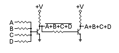
gates with multiple input resistors. Such a circuit is shown to the
right.
In this circuit, we have four input resistors. Raising any one input to
+5 volts will be sufficient to turn the transistor on, and applying
additional logic 1 (+5 volt) inputs will not really have any appreciable
effect on the output voltage. Remember that the forward bias voltage on
the transistor's base will not exceed 0.65 volt, so the current through a
grounded input resistor will not exceed 0.65v/15K = 0.04333 ma. This does
provide us with a practical limit on the number of allowable input
resistors to a single transistor, but doesn't cause any serious
problems.
The circuit shown here is a NOR/OR gate. That is, the basic gate is a
NOR gate, but an inverter is also included to provide an OR output as
well. This is often done with RTL circuits.
A NAND/AND equivalent should have the transistor's base biased on
through an extra input resistor, and use additional input resistors to
pull the transistor base down to ground. Unfortunately that won't work.
The same characteristics that allow multiple NOR inputs without mutual
interference prevent the use of NAND inputs. We just can't be sure of
draining enough current from the transistor's base to force the transistor
to turn off.
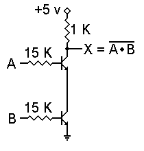
We can get a NAND function, however, in either of two ways. We can
simply invert the inputs to the NOR/OR gate, thus turning it into an
AND/NAND gate, or we can use the circuit shown to the left.
In this circuit, each transistor has its own separate input resistor,
so each is controlled by a different input signal. However, the only way
the output can be pulled down to logic 0 is if both transistors are turned
on by logic 1 inputs. If either input is a logic 0 that transistor cannot
conduct, so there is no current through either one. The output is then a
logic 1. This is the behavior of a NAND gate. Of course, an inverter can
also be included to provide an AND output at the same time.
The problem with this NAND circuit stems from the fact that transistors
are not ideal devices. Remember that 0.3 volt collector saturation
voltage? Ideally it should be zero. Since it isn't, we need to look at
what happens when we "stack" transistors this way. With two, the
combined collector saturation voltage is 0.6 volt -- only slightly less
than the 0.65 volt base voltage that will turn a transistor on.
If we stack three transistors for a 3-input NAND gate, the combined
collector sturation voltage is 0.9 volt. This is too high; it will promote
conduction in the next transistor no matter what. In addition, the load
presented by the upper transistor to the gate that drives it will be
different from the load presented by the lower transistor. This kind of
unevenness can cause some odd problems to appear, especially as the
frequency of operation increases.
Select another Logic Family you wish to examine:
[Diode Logic (DL)]
[Resistor-Transistor Logic (RTL)]
[Diode-Transistor Logic (DTL)]
[Transistor-Transistor Logic (TTL)]
[Emitter-Coupled Logic (ECL)]
[CMOS]
Go to the Logic Family base
page.
Go to the Logical Story pages.
Return to the Play-Hookey home page.