[Diode Logic (DL)]
[Resistor-Transistor Logic (RTL)]
[Diode-Transistor Logic (DTL)]
[Transistor-Transistor Logic (TTL)]
[Emitter-Coupled Logic (ECL)]
[CMOS]
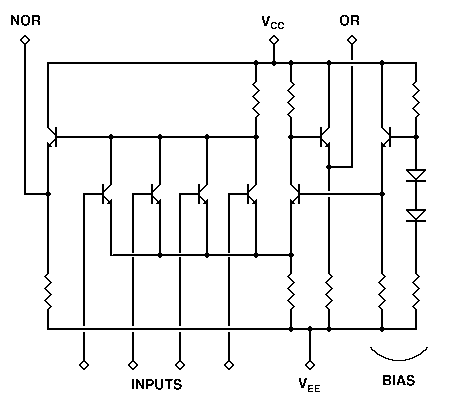
Emitter-Coupled Logic is based on the use of a multi-input differential amplifier to amplify and combine the digital signals, and emitter followers to adjust the dc voltage levels. As a result, none of the transistors in the gate ever enter saturation, nor do they ever get turned completely off. The transistors remain entirely within their active operating regions at all times. As a result, the transistors do not have a charge storage time to contend with, and can change states much more rapidly. Thus, the main advantage of this type of logic gate is extremely high speed.
The schematic diagram shown here is taken from Motorola's 1000/10,000 series of MECL devices. This particular circuit is of one 4-input OR/NOR gate. Standard voltages for this circuit are -5.2 volts (VEE) and ground (VCC). Unused inputs are connected to VEE. The bias circuit at the right side, consisting of one transistor and its associated diodes and resistors, can handle any number of gates in a single IC package. Typical ICs include dual 4-input, triple 3-input, and quad 2-input gates. In each case, the gates themselves differ only in how many input transistors they have. A single bias circuit serves all gates.
In operation, a logical ouput changes state by only 0.85 volt, from a low of -1.60 volts to a high of -0.75 volt. The internal bias circuit supplies a fixed voltage of -1.175 volts to the bias transistor in the differential amplifier. If all inputs are at -1.6 volts (or tied to VEE), the input transistors will all be off, and only the internal differential transistor will conduct current. This reduces the base voltage of the OR output transistor, lowering its output voltage to -1.60 volts. At the same time, no input transistors are affecting the NOR output transistor's base, so its output rises to -0.75 volt. This is simply the emitter-base voltage, VBE, of the transistor itself. (All transistors are alike within the IC, and are designed to have a VBE of 0.75 volt.)
When any input rises to -0.75 volt, that transistor siphons emitter current away from the internal differential transistor, causing the outputs to switch states.
The voltage changes in this type of circuit are small, and are dictated by the VBE of the transistors involved when they are on. Of greater importance to the operation of the circuit is the amount of current flowing through various transistors, rather than the precise voltages involved. Accordingly, Emitter-Coupled Logic is also known as Current Mode Logic (CML). This leads us to a major drawback of this type of gate: it draws a great deal of current from the power supply, and hence tends to dissipate a significant amount of heat.
To minimize this problem, some devices such as frequency counters use an ECL decade counter at the input end of the circuitry, followed by TTL or high-speed CMOS counters at the later digit positions. This puts the fast, expensive IC where it is absolutely required, and allows us to use cheaper ICs in locations where the signal will never be at that high a frequency.
[Diode Logic (DL)]
[Resistor-Transistor Logic (RTL)]
[Diode-Transistor Logic (DTL)]
[Transistor-Transistor Logic (TTL)]
[Emitter-Coupled Logic (ECL)]
[CMOS]
Go to the Logic Family base page.