The Clocked RS NAND Latch

Direct links to other logic pages:
Combinational Logic:
[Basic Gates]
[Derived Gates]
[The XOR Function]
[Binary Addition]
[Multiplexer]
[Decoder/Demultiplexer]
Sequential Logic:
[RS NAND Latch]
[Clocked RS Latch]
[RS Flip-Flop]
[JK Flip-Flop]
[D Latch]
[Flip-Flop Symbols]
Counters:
[Basic 4-Bit Counter]
Registers:
(Coming Soon)
Return to Digital index page.
Return to Play-Hookey Home Page.
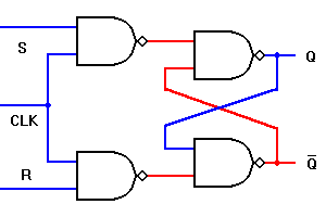
By adding a pair of NAND gates to the input circuits of the RS latch,
we accomplish two goals: normal rather than inverted inputs, and a third
input common to both gates which we can use to synchronize this circuit
with others of its kind.
The clocked RS NAND latch is shown below.


|
|
The clocked RS latch circuit is very similar in operation to the basic
latch you examined on the previous page. The S and R inputs are normally
at logic 0, and must be changed to logic 1 to change the state of the
latch. However, with the third input, a new factor has been added. This
input is typically designated C or CLK, because it is
typically controlled by a clock circuit of some sort, which is used to
synchronize several of these latch circuits with each other. The output
can only change state while the CLK input is a logic 1. When CLK is a
logic 0, the S and R inputs will have no effect.
The same rule about not activating both the S and R inputs
simultaneously holds true: if both are logic 1 when the clock is also
logic 1, the latching action is bypassed and both outputs will go to logic
1. The difference in this case is that if the CLK input drops to logic 0
first, there is no question or doubt -- a true race condition will exist,
and you cannot tell which way the outputs will come to rest. The example
circuit on this page reflects this uncertainty.
For correct operation, the selected R or S input should be brought to
logic 1, then the CLK input should be made logic 1 and then logic 0 again.
Finally, the selected input should be returned to logic 0.
|
The clocked RS latch solves some of the problems of basic RS latch
circuit, and allows closer control of the latching action. However, it is
by no means a complete solution. A major problem remaining is that this
latch circuit could easily experience a change in S and R input levels
while the CLK input is still at a logic 1 level. This allows the circuit
to change state many times before the CLK input returns to logic 0.
One way to minimize this problem is to keep the CLK at logic 0 most of
the time, and to allow only brief changes to logic 1. However, this
approach still cannot guarantee that the latch will only change state once
while the clock signal is at logic 1. This signal must have a certain
duration to make sure all latches have time to respond to it, and in that
time, most latches can respond to multiple changes.
A better way is to make sure that the latch can only change its outputs
at one instant of the clock cycle. The next page will demonstrate a
circuit which solves this problem handily, by changing states only on a
particular transistion, or edge, of the clock signal.
Back to the Play-Hookey main page.