|
|
 |
Combinational Logic:
[Basic Gates]
[Derived Gates]
[The XOR Function]
[Binary Addition]
[Multiplexer]
[Decoder/Demultiplexer]
Sequential Logic:
[RS NAND Latch]
[Clocked RS Latch]
[RS Flip-Flop]
[JK Flip-Flop]
[D Latch]
[Flip-Flop Symbols]
Counters:
[Basic 4-Bit Counter]
Registers:
(Coming Soon)
Return to Digital index page.
Return to Play-Hookey Home Page.
To adjust the clocked RS latch for edge triggering, we must actually combine two identical clocked latch circuits, but have them operate on opposite halves of the clock signal. The resulting circuit is commonly called a flip-flop, because its output can first flip one way and then flop back the other way. The clocked RS latch is also sometimes called a flip-flop, although it is more properly referred to as a latch circuit.
The two-section flip-flop is also known as a master-slave flip-flop, because the input latch operates as the master section, while the output section is slaved to the master during half of each clock cycle.
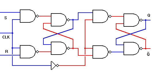
The edge-triggered RS NAND flip-flop is shown below.
|
|
 |
The edge-triggered RS flip-flop actually consists of two identical RS latch circuits, as shown above. However, the inverter connected between the two CLK inputs ensures that the two sections will be enabled during opposite half-cycles of the clock signal. This is the key to the operation of this circuit.
If we start with the CLK input at logic 0 as initially depicted above, the S and R inputs are disconnected from the input (master) latch. Therefore, any changes in the input signals cannot affect the state of the final outputs.
When the CLK signal goes to logic 1, the S and R inputs are able to control the state of the input latch, just as with the single RS latch circuit you already examined. However, at the same time the inverted CLK signal applied to the output (slave) latch prevents the state of the input latch from having any effect here. Therefore, any changes in the R and S input signals are tracked by the input latch while CLK is at logic 1, but are not reflected at the Q and Q' outputs.
When CLK falls again to logic 0, the S and R inputs are again isolated from the input latch. At the same time, the inverted CLK signal now allows the current state of the input latch to reach the output latch. Therefore, the Q and Q' outputs can only change state when the CLK signal falls from a logic 1 to logic 0. This is known as the falling edge of the CLK signal; hence the designation edge-triggered flip-flop.
By going to a master-slave structure and making the flip-flop edge-triggered, we have made sure that we can precisely control the moment when all flip-flops will change state. We have also allowed plenty of time for the master latch to respond to the input signals, and for those input signals to change and settle following the previous change of state.
There is still one problem left to solve: the possible race condition which may occur if both the S and R inputs are at logic 1 when CLK falls from logic 1 to logic 0. In the example above, we automatically assume that the race will always end with the master latch in the logic 1 state, but this will not be certain with real components. Therefore, we need to have a way to prevent race conditions from occurring at all. That way we won't have to figure out which gate in the circuit won the race on this particular occasion.
The solution is to add some additional feedback from the slave latch to the master latch. The resulting circuit is called a JK flip-flop.
|
|
|
|
| The Clocked RS Latch | Return to Digital Page | The JK Flip-Flop |