|
|
www.play-hookey.com | Mon, 08-26-2002 |
| Digital | Logic Families | Digital Experiments | Analog | Optics | Computers | Semiconductors | Test HTML | ||
| Direct Links to Other Semiconductors Pages: | |
|---|---|
| Basic Semiconductor Structures: | [Basic Semiconductor Crystal Structure] [The PN Junction] [The Transistor] |
| Field Effect Transistors (FETs): | [Junction FET] [Depletion Mode MOSFET] [Enhancement Mode MOSFET] |
| Adding More Junctions: | [The Four-Layer Diode] [The Silicon Controlled Rectifier] [The Silicon Controlled Switch] [The Diac and Triac] |
| Specialized Devices: | [A Touch of Physics] [Specialized Diodes] [The Unijunction Transistor] |
| The Four-Layer Diode |
|---|
If we add a junction to a transistor, we get a four-layer device. At irst glance, this may seem either useless or counter-productive, but this is not the case.

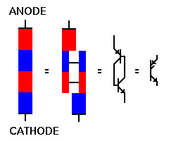
The diagram to the right shows the structure an nomenclature of the four-layer diode, together with its equivalent structure, showing its logical behavior, and its schematic symbol. Rather than acting simply as an odd sort of diode, this device actually behaves as two transistors, interconnected back-to-back as shown. The external connections are designated the cathode (n-type connection) and anode (p-type connection). This keeps us from having to distinguish between the n-emitter and the p-emitter.
In operation, the device is placed in a circuit so that the anode is held positive with respect to the cathode. If this voltage polarity is reversed, the four-layer diode exhibits two reverse-biased junctions and will not conduct current.
The applied voltage appears mainly across the reverse-biased center junction of the device, and the quiescent current flowing through the device is quite small, consisting essentially of a leakage current. As the applied voltage increases slowly, the leakage curent increases slowly as well, until the applied voltage reaches a certain level. At this voltage, known as the breakover voltage or firing voltage of the device, the two logical transistors both turn on and current increases dramatically. At the same time, the voltage across the diode decreases to almost zero, and the applied voltage now appears across whatever load circuit or device is connected in series with the diode. The diode has just switched from its off (or blocking) state to its on state.
Once the four-layer diode is conducting, it will continue to conduct as long as current continues to flow. It can only be turned off by reducing the circuit voltage and/or current to below the leves required to sustain conduction. Typically, this means either removing power totally from the circuit, or else using the diode as a device to periodically discharge a capacitor.
The breakover voltage and current-handling capacity of a given four-layer diode are determined by the exact details of its manufacture. Four-layer diodes may be manufactured with a wide range of voltage and current ratings.
There is one problem which can appear with the four-layer diode: if the applied voltage rises rapidly, the inherent capacitance associated with the reverse-biased middle junction will transmit the applied voltage more directly, and cause the diode to switch on at a voltage well below its designed breakover voltage. This phenomenon is known as the rate effect.
Applications for the four-layer diode fall into two categories. In active cirucits, they can be used as the active element in a sawtooth waveform generator or triggered pulse generator. Or, they can be used as a "crowbar" element in a power supply. In this last application, the four-layer diode is placed directly across the output terminals of the power supply, used to power delicate circuitry. If the supply voltage should rise for any reason to a level that might damage the circuitry, the four-layer diode breaks over and draws a heavy current from the supply. This overloads the supply and causes the fuse or circuit breaker to blow. It's a drastic measure, but still much better than allowing expensive circuit components to be damaged or destroyed.
|
|
|
|
|
All pages on www.play-hookey.com copyright © 1996, 2000-2002 by
Ken Bigelow Please address queries and suggestions to: webmaster@play-hookey.com |