|
|
www.play-hookey.com | Mon, 08-26-2002 |
| Digital | Logic Families | Digital Experiments | Analog | Optics | Computers | Semiconductors | Test HTML | ||
| Direct Links to Other Semiconductors Pages: | |
|---|---|
| Basic Semiconductor Structures: | [Basic Semiconductor Crystal Structure] [The PN Junction] [The Transistor] |
| Field Effect Transistors (FETs): | [Junction FET] [Depletion Mode MOSFET] [Enhancement Mode MOSFET] |
| Adding More Junctions: | [The Four-Layer Diode] [The Silicon Controlled Rectifier] [The Silicon Controlled Switch] [The Diac and Triac] |
| Specialized Devices: | [A Touch of Physics] [Specialized Diodes] [The Unijunction Transistor] |
| The Depletion Mode MOSFET |
|---|
In the page on junction FETs, we noted that the electric field associated with a reverse-biased pn junction creates a depletion region within the channel, which restricts the flow of electricity through the channel. The stronger the field, the larger the depletion zone, and the greater the restriction of the channel.
However, an electric field is associated with any electrical charge, and not only with a pn junction. Can we then take our channel and somehow just use a metal gate, while insulating the gate from the channel? Let's see what happens when we try.
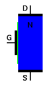
First, we note that the main ingredient of the channel is silicon. It can be a p-type or n-type channel; it is still mostly silicon. Next, we take note that silicon dioxide is simply glass, which is a good insulator. So we can form a thin layer of silicon dioxide along one surface of the channel, and then lay our metal gate region down over the glass. The result is shown to the left.
This device is sometimes known as an insulated-gate field effect transistor, or IGFET. More commonly, noting the construction of the gate, it is called a metal-oxide-semiconductor FET, or MOSFET.
With no voltage applied to the gate (G) electrode, the channel really is just a semiconductor resistance, and will conduct current according to the voltage applied between source (S) and drain (D). There is no pn junction, so there is no depletion region.
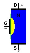
With an appropriate voltage applied between source and drain, current will flow through the channel, as a semiconductor resistance. However, if we now apply a negative voltage to the gate, asd shown to the right, it will amount to a small negative static charge on the gate. This negative voltage will repel electrons, with their negative charge, away from the gate. But free electrons are the majority current carriers in the n-type silicon channel. By repelling them away from the gate region, the applied gate voltage creates a depletion region around the gate area, thus restricting the usable width of the channel just as the pn junction did.
Because this type of FET operates by creating a depletion region within an existing channel, it is called a depletion-mode MOSFET.
The basic advantage of the MOSFET is that it draws no gate current at all; not even a leakage current. Thus, the input resistance of this device is essentially infinite. However, that also leads to a couple of disadvantages: that thin layer of glass can't withstand much voltage; even the static charge you can build on your body walking across a rug when the air is dry is enough to destroy the device if it isn't mounted in a circuit that will drain off the charge. To prevent such damage, individual MOSFETs are typically packaged in metal cans with four leads (the fourth lead connected to the can itself. The four leads are conneted by a wire ring around them, which remains in place until the device is installed in its circuit. Then it can be cut away safely.
The second disadvantage has to do with the inherent capacitance between the gate and the channel. It may not seem like much, but it does limit the frequency response in analog circuits, or the maximum switching speed in digital circuits.
|
|
|
|
|
All pages on www.play-hookey.com copyright © 1996, 2000-2002 by
Ken Bigelow Please address queries and suggestions to: webmaster@play-hookey.com |