|
|
www.play-hookey.com | Mon, 08-26-2002 |
| Digital | Logic Families | Digital Experiments | Analog | Optics | Computers | Semiconductors | Test HTML | ||
| Direct Links to Other Semiconductors Pages: | |
|---|---|
| Basic Semiconductor Structures: | [Basic Semiconductor Crystal Structure] [The PN Junction] [The Transistor] |
| Field Effect Transistors (FETs): | [Junction FET] [Depletion Mode MOSFET] [Enhancement Mode MOSFET] |
| Adding More Junctions: | [The Four-Layer Diode] [The Silicon Controlled Rectifier] [The Silicon Controlled Switch] [The Diac and Triac] |
| Specialized Devices: | [A Touch of Physics] [Specialized Diodes] [The Unijunction Transistor] |
| The Transistor |
|---|
While a single PN junction is useful, it also has its limitations. It can either conduct currrent or not, but can't really control how much current it will conduct.
So what happens if we add a second junction? Can we play around with that idea and see where it goes?

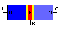
A basic two-junction semiconductor must necessarily have one type of region sandwiched between two of the other type. To the right is an example of a semiconductor device consisting of a narrow P-type region between two N-type regions. For reasons we will see shortly, the three regions are designated the emitter (E), base (B), and collector (C), respectively. In modern versions of this device, the emitter region is heavily doped with the appropriate impurity, while the base region is very lightly doped. The collector region has a moderate doping level so it will have a low internal resistance.
We have shown a device consisting of N, P, and N regions in order, but there is no reason not to build equivalent devices in P, N, and P order instead. In fact, it is often very useful to have both types of devices available.
With no electrical voltages applied, of course, this semiconductor will of course just sit there and do nothing. So let's move forward and see what happens when we apply bias voltages to the device.

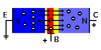
To the left we see the same semiconductor device as above, with a small forward bias applied to the emitter-base junction, and a larger reverse bias applied to the collector-base junction. As we will see, these are the normal operating conditions of this device.
Since we already know how a single-junction device, the diode, behaves, we would normally expect the base voltage to be about 0.65 to 0.7 volt positive with respect to the emitter, and to have electrons move from emitter to base, and leave the device at that point. With the collector junction reverse biased, we would expect no current to flow through that junction.
But a funny thing happens inside the base region. The forward bias on this junction does indeed attract electrons from the emitter into the base, but there the forward momentum of the electrons carries them across most of the base region and into the depletion region around the collector junction. From there, the higher positive collector voltage attracts these electrons across the collector junction and into the collector region. (Remember that the electrons are minority current carriers within the P-type pase region, and can therefore cross the reverse-biased junction as a leakage current.)
A small amount of current does still leave the device through the base contact, but most of the current is diverted through the collector instead. In this way, the small base bias current controls the much larger collector current. If a small varying current is applied to the base along with the bias, the collector current will vary to a much greater degree. Thus, this device can not only be used to control a varying signal; it can amplify that signal as well.
Because of the way this device operates to transfer current (and its internal resistances) from the original conduction path to another, it's name is a combination of the words "transfer" and "resistor:" transistor.

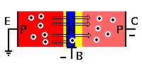
It's also quite possible to build a transistor with the region types reversed, as shown to the right. In this case, holes will be drawn from the emitter into the base region by the forward bias, and will then be pulled into the collector region by the higher negative bias. Otherwise, this device works the same way and has the same general properties as the one described above.
To distinguish between the two types of transistors, we refer to them by the order in which the different regions appear. Thus, this is a PNP transistor while the device described above is an NPN transistor.
|
|
|
|
|
All pages on www.play-hookey.com copyright © 1996, 2000-2002 by
Ken Bigelow Please address queries and suggestions to: webmaster@play-hookey.com |