|
|
www.play-hookey.com | Mon, 08-26-2002 |
| Digital | Logic Families | Digital Experiments | Analog | Optics | Computers | Semiconductors | Test HTML | ||
| Direct Links to Other Semiconductors Pages: | |
|---|---|
| Basic Semiconductor Structures: | [Basic Semiconductor Crystal Structure] [The PN Junction] [The Transistor] |
| Field Effect Transistors (FETs): | [Junction FET] [Depletion Mode MOSFET] [Enhancement Mode MOSFET] |
| Adding More Junctions: | [The Four-Layer Diode] [The Silicon Controlled Rectifier] [The Silicon Controlled Switch] [The Diac and Triac] |
| Specialized Devices: | [A Touch of Physics] [Specialized Diodes] [The Unijunction Transistor] |
| The Junction FET |
|---|

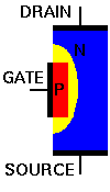
Suppose we take a basic pn junction and change its shape. Let's enlarge the n-type section and make two connections to it, thus treating it essentially as a semiconductor resistance. However, we will also leave the pn junction in place, centered along the n-type section as showm. The n-type section is known as the channel, and the two ends are known as the source and drain. The connection to the p-type region is known as the gate, for reasons that we will see shortly.
The depletion region at the junction spreads into the channel as shown. If no voltage is applied to any part of the device, the depletion region remains of a moderate size, and of course no current flows through any part of the device.
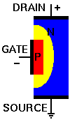
In normal usage, a voltage is applied across the channel, with the drain being made positive with respect to the source. Thus, electrons will move through the n-type channel from source to drain, with the applied voltage and the resistance of the channel determining the magnitude of current flowing, in accordance with Ohm's Law. There is one caveat to this, however: the depletion region in the middle of the channel will not carry current. Therefore, the effective width of the channel is restricted by the depleion region, and its effective resistance is higher in this part of the channel, than in any other part of the channel.

If the gate becomes forward biased with respect to the channel, of course, the depletion region shrinks away and no longer controls the flow of current through the channel. This is not generally useful in practical electronic circuits.
However, if the gate becomes reverse biased with respect to the channel, the applied electric field will enlarge the depletion region, as shown to the left. As a result, the working channel width is reduced, and the effective channel resistance is increased significantly. In this manner, a small voltage applied to the gate can have a profound effect on the current flowing through the channel. Indeed, if the applied reverse bias becomes high enough, the depletion region can cover the entire width of the channel, and cut off current flow completely.
Because the electric field produced by the applied gate voltage controls the resistance of the channel (and therefore the current flowing through the channel), this device is known as a field-effect transistor (FET). In addition, because the control voltage at the gate is applied to a pn junction, and because the channel is made of n-type semiconductor material, the device is properly called an n-channel junction field-effect transistor, or n-channel JFET.
It is quite possible to reverse the semiconductor regions, in which case we would have a p-channel JFET. Of course, the applied voltages must be reversed in polarity for a p-channel device, and the current carriers withing the p-type channel are holes rather than electrons. Otherwise, the basic behavior of the device is the same.
If the channel has a uniform concentration of impurities and the gate is placed in the middle of the channel, the FET is said to by symmetrical. In this case, the source and drain are interchangeable, which can be useful in some applications. However, many FETs are deliberately constructed to be unsymmetrical, to enhance certain parameters and behaviors. In these FET types, performance will be impaired if source and drain are interchanged.
JFETs, like any semiconductor device, have their advantages and disadvantages. Since they are controlled by the applied gate voltage, they draw no gate current (except for a small leakage current, which can be a disadvantage), and hence present a very high input resistance to any signal source. In addition, the reverse-biased junction can take a considerable amount of radiation damage without any appreciable change to the FET operation. This makes the JFET an excellent choice for operation in high-radiation environments.
|
|
|
|
|
All pages on www.play-hookey.com copyright © 1996, 2000-2002 by
Ken Bigelow Please address queries and suggestions to: webmaster@play-hookey.com |