|
|
www.play-hookey.com | Mon, 08-26-2002 |
| Digital | Logic Families | Digital Experiments | Analog | Optics | Computers | Semiconductors | Test HTML | ||
| Direct Links to Other Semiconductors Pages: | |
|---|---|
| Basic Semiconductor Structures: | [Basic Semiconductor Crystal Structure] [The PN Junction] [The Transistor] |
| Field Effect Transistors (FETs): | [Junction FET] [Depletion Mode MOSFET] [Enhancement Mode MOSFET] |
| Adding More Junctions: | [The Four-Layer Diode] [The Silicon Controlled Rectifier] [The Silicon Controlled Switch] [The Diac and Triac] |
| Specialized Devices: | [A Touch of Physics] [Specialized Diodes] [The Unijunction Transistor] |
| The Enhancement Mode MOSFET |
|---|
Both the junction FET and the depletion mode MOSFET operate in a generally intuitive manner. In both device types, an electric field is used to deplete the channel of current carriers to one degree or another, so that a control voltage will directly affect and control the amount of current flowing through the channel. But what happens if we have a device with no working channel, but with room to put a channel in place. Can we generate a channel electrically?
NOTE: The device described on this page is not generally used or manufactured as a separate device. Rather, it is one of many such devices manufactured in tandem as parts of an integrated circuit. However, each such device is still an entity unto itself, so we will look at just one such device, and examine it by itself.
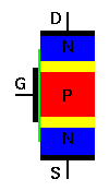
The mechanical structure of this device is shown to the right. In an IC, we would place two n-type regions side by side within a p-type area and then place the gate between the n-type regions. However, the important region still consists of the two n-type regions and the p-type area between them. This is the portion we have depicted to the right.
With no applied bias, we have what amounts to an npn transistor with no base connection. The two n-type regions are isolated from each other, and are electrically separate. Even with a voltage applied between the two n-type regions, there is no channel present and no current flow.
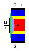
While we still apply the usual positive voltage to the drain with respect to the source, this time we will also apply a positive voltage to the gate region. This has the effect of attracting free electrons towards the gate. The larger the positive gate voltage, the wider its electric field and the more free electrons it will attract.
You might not think this would have any effect on the p-type region, where the majority current carriers are holes. However, there are some free electrons here as well. In addition, the source junction is forward biased, so the positive gate voltage can attract electrons across this junction towards the gate.
The net result is that the electrons attracted towards the gate actually enhance a channel within the p-type region, as shown to the left. This is a channel formed of free electrons, and actually bridges the gap between source and drain. Now we have a channel, which can conduct current from source to drain through the device.
Because these devices operate by having a channel enhanced in the semiconductor material where no channel was constructed, they are known as enhancement-mode MOSFETs. It is just as easy to construct p-channel versions of these devices as n-channel versions. Indeed CMOS logic ICs consist of nothing but these devices, constructed and used in pairs such that one will be turned off while the other is turned on. This is the source of the designation CMOS: Complementary MOS.
Enhancement-mode MOSFETs have the same advantages and disadvantages as their depletion-mode cousins. However, since they are constructed as part of an IC rather than as individual devices, they are not readily subject to random static charges. The ICs are constructed with input protection circuitry for any MOSFET input that must be made accessible to external circuitry.
|
|
|
|
|
All pages on www.play-hookey.com copyright © 1996, 2000-2002 by
Ken Bigelow Please address queries and suggestions to: webmaster@play-hookey.com |