|
|
www.play-hookey.com | Mon, 08-26-2002 |
| Digital | Logic Families | Digital Experiments | Analog | Optics | Computers | Semiconductors | Test HTML | ||
| Direct Links to Other Semiconductors Pages: | |
|---|---|
| Basic Semiconductor Structures: | [Basic Semiconductor Crystal Structure] [The PN Junction] [The Transistor] |
| Field Effect Transistors (FETs): | [Junction FET] [Depletion Mode MOSFET] [Enhancement Mode MOSFET] |
| Adding More Junctions: | [The Four-Layer Diode] [The Silicon Controlled Rectifier] [The Silicon Controlled Switch] [The Diac and Triac] |
| Specialized Devices: | [A Touch of Physics] [Specialized Diodes] [The Unijunction Transistor] |
| The Unijunction Transistor |
|---|
One of the oddest semiconductor devices in use is the unijunction transistor (UJT). As its name suggests, this is a three-terminal device which nevertheless has only one PN junction. It cannot amplify an applied signal, but it nevertheless can be used as the active element in an oscillator circuit.
The figure to the right shows the physical construction of a typical UJT. It consists of a bar of N-type silicon with electrical connections at either end, plus an aluminum wire bonded to a point along the length of the silicon bar. At the bonding point, the aluminum creates a P-type region in the silicon bar, thus forming a PN junction.
Because there's only one junction, it's not reasonable to use the terms anode or cathode, so designations are taken instead from transistor notations. The P-type connection is known as the "Emitter," while the two N-type connections are designated "Base 1" and "Base 2." For this reason, the device is sometimes called a "double-base diode."

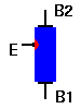
The schematic symbol for the UJT appears to the right. The symbol actually represents the construction of the UJT, as shown above, quite well.
In use, an appropriate bias voltage is applied between the two bases, with B2 made positive with respect to B1. Because the N-type bar is resistive, a relatively small current will flow through it, and the applied voltage will be distributed evenly along its length. If we start with the Emitter grounded, the junction will be reverse biased and there will be no emitter current. As the emitter voltage increases, there is no change until the junction suddenly becomes forward biased.
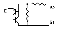
At this point, the emitter injects holes into the silicon bar, greatly reducing the effective resistance of the bar between E and B1. This will lower the emitter voltage required to keep the junction forward biased, and will sustain a heavy emitter current. This condition will continue as long as the circuit connected to the emitter can sustain the heavier current flow. The UJT thus behaves like a variation of the SCR, as suggested by the equivalent circuit shown to the right.

It is also possible to build a UJT with a P-type silicon bar and an N-type emitter. It isn't used as commonly, but has been constructed. It is known as a complementary UJT (CUJT); its schematic symbol is shown to the right. The CUJT behaves the same as the UJT, but with reversed voltage polarities.
|
|
|
|
|
All pages on www.play-hookey.com copyright © 1996, 2000-2002 by
Ken Bigelow Please address queries and suggestions to: webmaster@play-hookey.com |