|
|
www.play-hookey.com | Mon, 08-26-2002 |
| Digital | Logic Families | Digital Experiments | Analog | Optics | Computers | Semiconductors | Test HTML | ||
| Direct Links to Other Semiconductors Pages: | |
|---|---|
| Basic Semiconductor Structures: | [Basic Semiconductor Crystal Structure] [The PN Junction] [The Transistor] |
| Field Effect Transistors (FETs): | [Junction FET] [Depletion Mode MOSFET] [Enhancement Mode MOSFET] |
| Adding More Junctions: | [The Four-Layer Diode] [The Silicon Controlled Rectifier] [The Silicon Controlled Switch] [The Diac and Triac] |
| Specialized Devices: | [A Touch of Physics] [Specialized Diodes] [The Unijunction Transistor] |
| A Touch of Physics |
|---|
In order to understand how diodes can have very different properties according to how they are manufactured, it is necessary to first delve a bit into the physics involved. Don't worry; we won't get any deeper in than we have to, but we have to use this method to understand the differences between different kinds of diodes, and why they can do to odd (and useful) things they do.

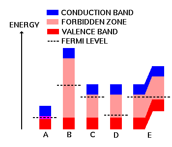
Consider the diagram to the right. This figure shows the important range of electron energy in four different kinds of materials. To understand this diagram, let's define a few terms.
Diagram A above represents a good conductor, such as copper or silver. Here, at temperatures above Absolute Zero, electrons are always available to conduct electrical current, even with no applied energy. In metals, the valence and conduction bands actually overlap.
Diagram B shows a typical insulator, such as glass. All electrons are pretty much locked into the atomic structure, and are unavailable as current carriers. It will take a lot of energy to break any electrons loose for conduction. It's not impossible (a lightning bolt can go through almost anything), but it takes a lot of applied energy.
Diagram C represents a crystal of N-type silicon (or germanium). The forbidden zone is still present, but much smaller than for an insulator. That's why this type of material is called a "semiconductor." With the crystal doped with N-type impurities, there are lots of electrons around with almost enough energy to roam freely, so the Fermi level gets pushed up close to the conduction band. If the doping level is heavy enough (large dosage of impurities), the Fermi level can actually enter the conduction band.
Diagram D represents a P-type semiconductor crystal. Here, the p-type impurities have left holes in the atomic structure, which tend to attact and hole free electrons. This pulls the Fermi level down until it gets close to the valence band. Similar to the highly-doped N-type crystal, a highly-doped P-type crystal will have its Fermi level within the valence band instead of just above it.
There are two important factors regarding the Fermi level in semiconductors. First, since the Fermi level is close to one of the working energy levels, it requires very little energy to push an electron over the edge and make it available for conduction. In an N-type crystal, only a very small applied voltage will kick the free electrons up into the conduction band to carry a current. In a P-type crystal, a small amount of energy will kick a bound electron just over the Fermi level into the forbidden zone. This doesn't make the electron available for bulk conduction, but does allow the applied voltage to push the eletron over into a hole, causing it to leave another hole behind it. In this way, a series of electrons can "hop" from bound state to bound state in a new location, allowing the hole to appear to move in the opposite direction. This is another way to think of hole conduction in semiconductor crystals.
The second factor to remember is that when a PN junction is formed in a single silicon or germanium crystal, the entire crystal as a whole has one Fermi level (see Diagram E above). The conduction and valence bands have differing energy levels across the crystal. As a result, the N-type conduction band is very close in energy to the P-type valence band. The transition region corresponds to the depletion region within the crystal. This is a major factor in the operation of all semiconductor devices, and helps to explain how we can get specific properties from a given device, according to just how we manufacture the semiconductor crystal.
|
|
|
|
|
All pages on www.play-hookey.com copyright © 1996, 2000-2002 by
Ken Bigelow Please address queries and suggestions to: webmaster@play-hookey.com |