|
|
www.play-hookey.com | Mon, 08-26-2002 |
| Digital | Logic Families | Digital Experiments | Analog | Optics | Computers | Semiconductors | Test HTML | ||
| Direct Links to Other Semiconductors Pages: | |
|---|---|
| Basic Semiconductor Structures: | [Basic Semiconductor Crystal Structure] [The PN Junction] [The Transistor] |
| Field Effect Transistors (FETs): | [Junction FET] [Depletion Mode MOSFET] [Enhancement Mode MOSFET] |
| Adding More Junctions: | [The Four-Layer Diode] [The Silicon Controlled Rectifier] [The Silicon Controlled Switch] [The Diac and Triac] |
| Specialized Devices: | [A Touch of Physics] [Specialized Diodes] [The Unijunction Transistor] |
| Basic Semiconductor Crystal Structure |
|---|
To understand how diodes, transistors, and other semiconductor devices can do what they do, it is first necessary to understand the basic structure of all semiconductor devices. Early semiconductors were fabricated from the element Germanium, but Silicon is preferred in most modern applications.
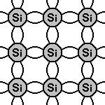
The crystal structure of pure silicon is of course 3-dimensional, but that is difficult to display or to see, so the image to the left is often used to represent the crystal structure of silicon. For you physics types, silicon (and germanium) falls in column IVa of the Periodic Table. This is the carbon family of elements. The essential characteristic of these elements is that each atom has four electrons to share with adjacent atoms in forming bonds.
While this is an oversimplified description, the nature of a bond between two silicon atoms is such that each atom provides one electron to share with the other. The two electrons thus shared are in fact shared equally between the two atoms. This type of sharing is known as a covalent bond. Such a bond is very stable, and holds the two atoms together very tightly, so that it requires a lot of energy to break this bond.
For those who are interested, the actual bonds in a 3-dimensional silicon crystal are arranged at equal angles from each other. If you visualize a tetrahedron (a pyramid with three points on the ground and a fourth point sticking straight up) with the atom centered inside, the four bonds will be directed towards the points of the tetrahedron.
Now we have our silicon crystal, but we still don't have a semiconductor. In the crystal we saw above, all of the outer electrons of all silicon atoms are used to make covalent bonds with other atoms. There are no electrons available to move from place to place as an electrical current. Thus, a pure silicon crystal is quite a good insulator. In fact, it is almost glass, which is silicon dioxide. A crystal of pure silicon is said to be an intrinsic crystal.
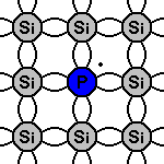
To allow our silicon crystal to conduct electricity, we must find a way to allow some electrons to move from place to place within the crystal, in spite of the covalent bonds between atoms. One way to accomplish this is to introduce an impurity such as Arsenic or Phosphorus into the crystal structure, as shown to the right. These elements are from column Va of the Periodic Table, and have five outer electrons to share with other atoms. In this application, four of these five electrons bond with adjacent silicon atoms as before, but the fifth electron cannot form a bond. This electron can easily be moved with only a small applied electrical voltage. Because the resulting crystal has an excess of current-carrying electrons, each with a negative charge, it is known as "N-type" silicon.
This construction does not conduct electricity as easily and readily as, say, copper or silver. It does exhibit some resistance to the flow of electricity. It cannot properly be called a conductor, but at the same time it is no longer an insulator. Therefore, it is known as a semiconductor.
While this effect is interesting, it still isn't particularly useful by itself. A plain carbon resistor is easier and cheaper to manufacture than a silicon semiconductor one. We still don't have any way to actually control an electrical current.
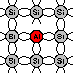
But wait a moment! We obtained a semiconductor material by introducing a 5-electron impurity into a matrix of 4-electron atoms. (For you physics types, we're only looking at the outer electrons that are available for bonding -- electrons in inner shells are not included in the process or in this discussion.) What happens if we go the other way, and introduce a 3-electron impurity into such a crystal. Suppose we introduce some Aluminum (from column IIIa in the Periodic Table) into the crystal, as shown to the left? We could also try Gallium, which is also in column IIIa right under aluminum. Now what?
These elements only have three electrons available to share with other atoms. Those three electrons do indeed form covalent bonds with adjacent silicon atoms, but the expected fourth bond cannot be formed. A complete connection is impossible here, leaving a "hole" in the structure of the crystal.
Experimentation shows that there is an empty place where an electron should logically go, and often an electron will try to move into that space to fill it. However, the electron filling the hole had to leave a covalent bond behind to fill this empty space, and therefore leaves another hole behind as it moves. Yet another electron may move into that hole, leaving another hole behind, and so forth. In this manner, holes appear to move as positive charges through the crystal. Therefore, this type of semiconductor material is designated "P-type" silicon.
By themselves, P-type semiconductors are no more useful than N-type semiconductors. The truly interesting effects begin when the two are combined in various ways, in a single crystal of silicon. The most basic and obvious combination is a single crystal with an N-type region at one end and a P-type region at the other. A crystal with two regions as described is known as a semiconductor diode, and is the topic of the next page.
|
|
|
|
|
All pages on www.play-hookey.com copyright © 1996, 2000-2002 by
Ken Bigelow Please address queries and suggestions to: webmaster@play-hookey.com |